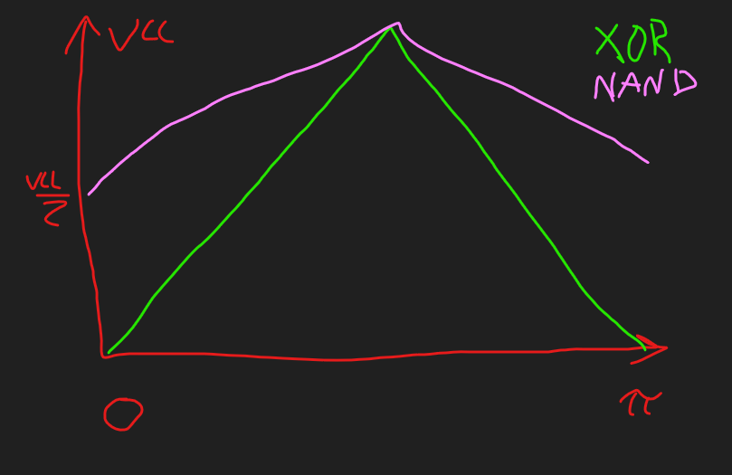
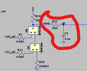
It isn’t but it does require many fewer transistors. Two, to be precise. The only difference between a NAND gate as a phase detector and an XOR gate is this:
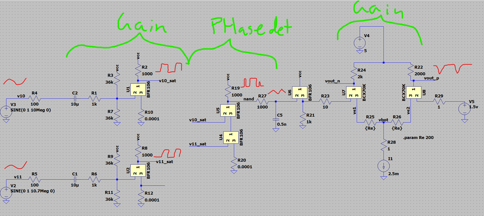
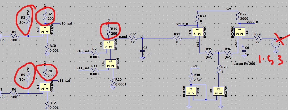
Which actually works just fine for me, since I was having lots of trouble making an amplifier where the input goes down to the negative rail. The whole thing put together in the simulation looks like this:
(Commit hash: eac9e150ca7f149b245ef8dea28d842c9a3f5f63)
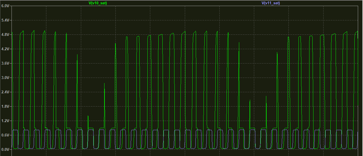
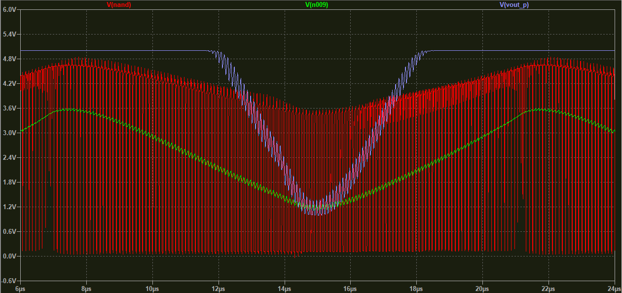
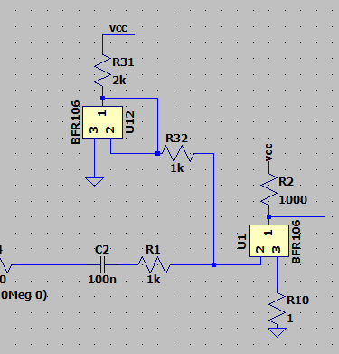
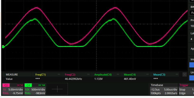
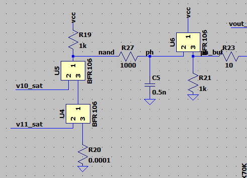
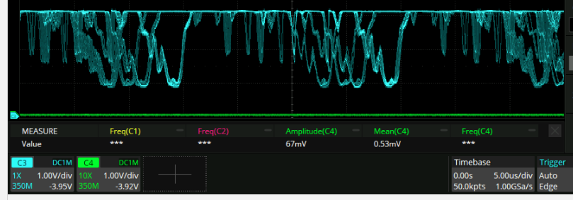
The two input transistors are responsible for providing a bunch of gain to make the output a nice big square wave. That goes into the NAND phase detector, which then goes into a diff amp. The saturated output of the first gain stage looks like this:
The second one isn’t very high amplitude cause it’s going straight into the base of the bottom transistor. The NAND output looks like this:
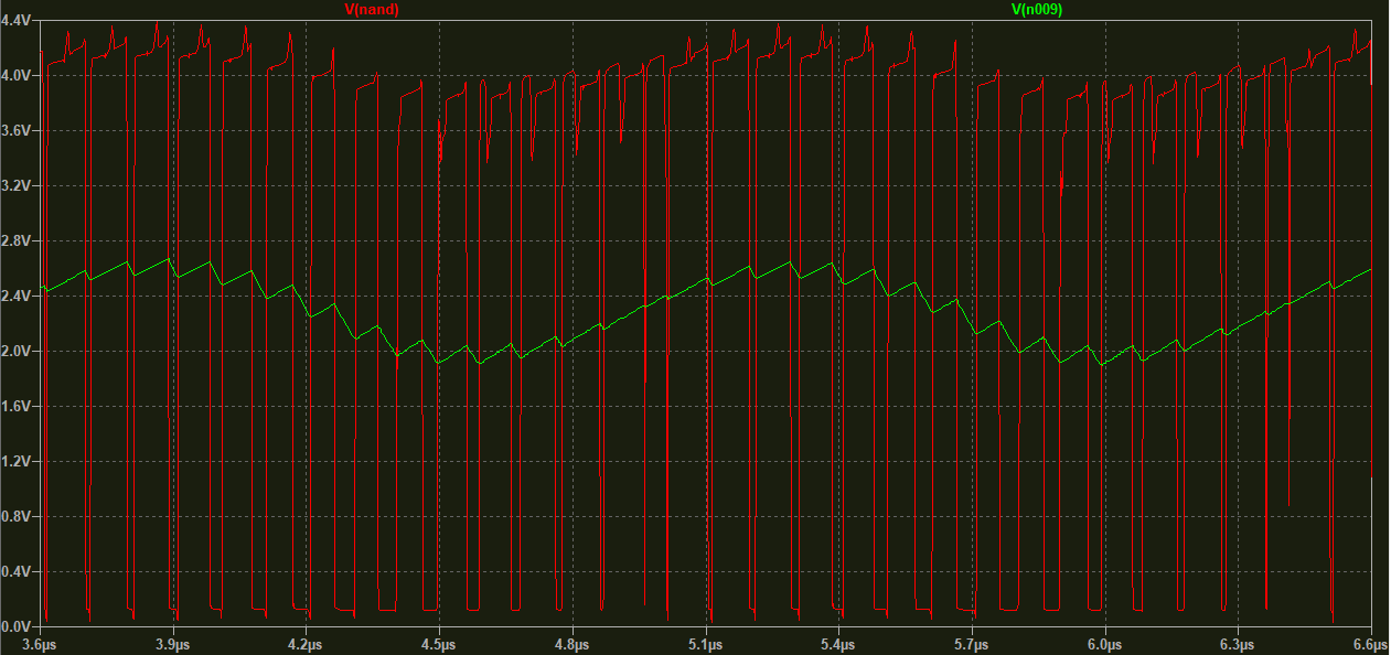
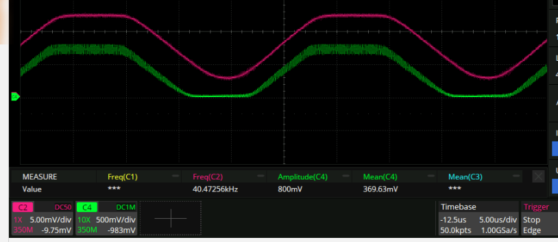
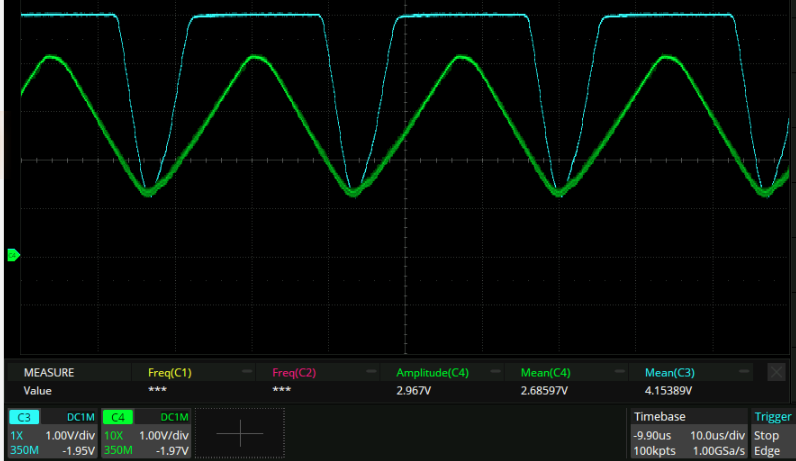
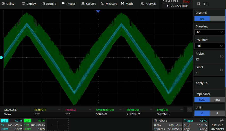
Before/after filtering. And then with gain it looks like this (I reduced the frequency difference by 10x here):
I made the gain of the diff amp about the same as last time (just under 10x) but I think it might need more this time because the phase detector output is lower amplitude by quite a bit. We’ll see.
Current source
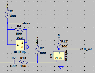
The art of electronics comes to the rescue as usual with a “current mirror” as a great programmable current source:
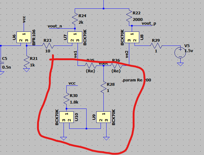
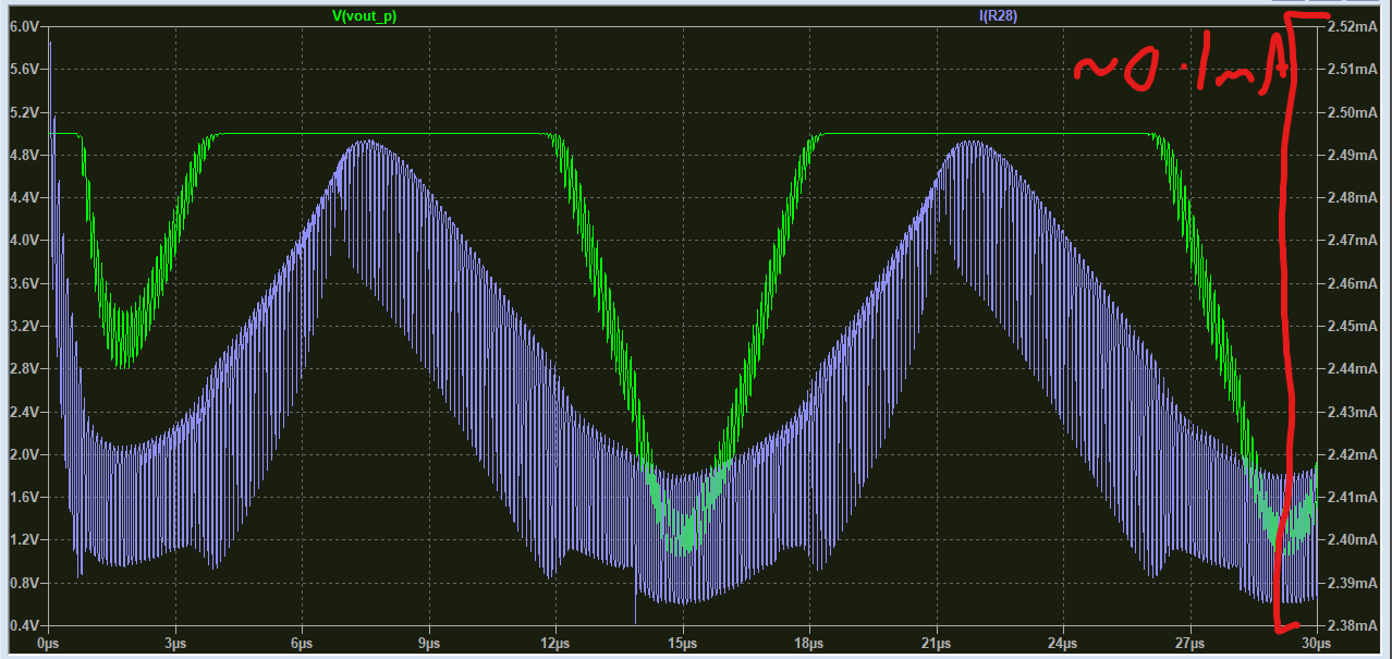
Remembering that according to the ebers-moll model of a transistor the collector current of a bjt is programmed according to the base-emitter voltage of the transistor. R30 sets the collector current of U10 (and thus also it’s base voltage) and then the base voltage of U10 is connected to U9’s base, thus also programming it’s collector current, the currentwe actually care about. This seems to work pretty well:
I think this has gotten good enough that it’s time to build it!
Preliminary problems
The output of the buffer (REF1) has too low of a duty cycle. I attribute this to the output of the buffer having too high of a duty cycle, and that being because it’s hitting the rail. So I should reduce the biasing on the base of that transistor. Because this transistor is intended to operate rail to rail (high gain) I think we have fallen into the trap of having a circuit that depends on a particular value of transistor gain. Maybe biasing all the amplifiers with current mirrors would work well, like this:
Since we already have a current mirror we can amortise the cost of this transitor across all the places we need a bias!
Aside: probing
Probing the collector of U1 above is a bit tricky by default for a 10MHz signal. Even 10pF of capacitance changes the output quite a bit, and a cable can have 100pF+! So putting a 50kr resistor out from the collector of the transistor and 50R terminating at the scope gets rid of the vast majoraity of the capacitance. The signal amplitude isn’t too bad either since it was originally 5vpp.
Phase output offset
It seems that the phase output doesn’t match the simulation, the output is too close to ground. It’s 0→XXXV rather than vcc/2→vcc. This means that things clip after the buffer because of the drop.
I don’t know why exactly. Decreasing R19 here to 100R improves the offset but it looks like the phase clips at the top and bottom of the range now:
Green: ‘ph_buf’ node (after U6 buffer) Pink: ‘ph’ node. So the goal here would be to reduce the quiescent current of U6. We can do this by:
- Increasing R27 ( changes loop filter rolloff)
- Putting new resistor from U6base to ground (also degrades signal)
- Increasing the bias on U1/U2 so that they have lower output current into the NAND gate. The whole biasing scheme of these tranistors seem bad but I applied the heat gun and nothing much happened.
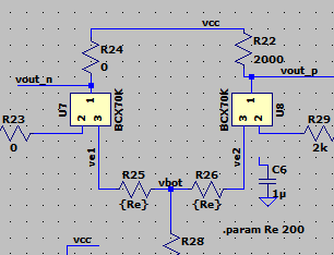
Instead of doing the above I changed component values to the following (Notice how I got rid of the buffer):
This leads to the following output:
Which is great! The minimum output voltage from the diff amp is about 1.2V but that was always the plan. Just put a diode or two on the output and voila!
Diode on the output
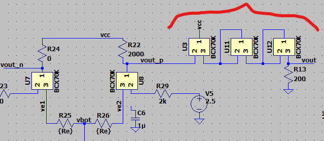
About 3 diode drops are needed in order to get an output that goes to the negative rail. But if you do that there’s a bunch of capacitance and whatnot and the bandwidth is garbage (I think). So instead just doing an emitter follower with some exta npn’s in the way is the way to go:
Which produces this waveform:
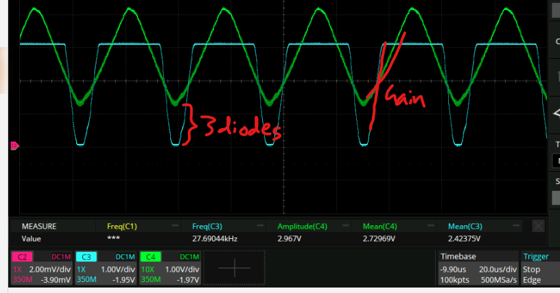
Where green is the vout_p node and blue is the vout node. I think this means that it’s ready for prime time in a loop! (A crude measurement indicates it has a 150kHz 3dB bandwidth. This actually seems to be limited by something upstream. Gee, that wouldn’t be R27/C5 would it?)
Prime time
Problem 1
I noticed that closing the loop switch caused one of the oscillators to stop oscillating. The control output was at the positive rail (3Vish cause of diode drop) when this happened. I adjusted the pots connected to the varactor diodes for each oscillator to ~2V/11.1MHz. This caused the DC level of the phase detector to shift a lot!
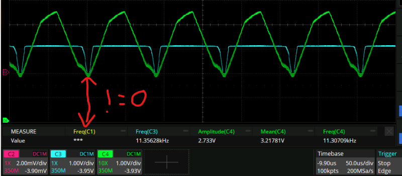
I think this is happening because there is an amplitude-frequency dependence to the VCO and this translates to a frequency-duty cycle dependence on the input to the NAND gate. Since the phase is the lowpassed version of the output of the NAND gate, the duty cycle of the input is very important. Perhaps this means that my gung ho “36k to the rail” transistor biasing was just as terrible as I’d feared. It should be possible to get it to the point where there is a 50% duty cycle output even with changes in the amplitude of the input.
Attempt #1: biasing
Here is how the art of electronics says you should bias a common emitter amplifier with a second transistor:
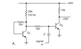
This looks like the regular current mirror that was used on the diff amp:
except for the addition of the resistors. Those resistors are there because unlike before you can’t connect the bases directly together (that would wreck the input impedance). Works great:

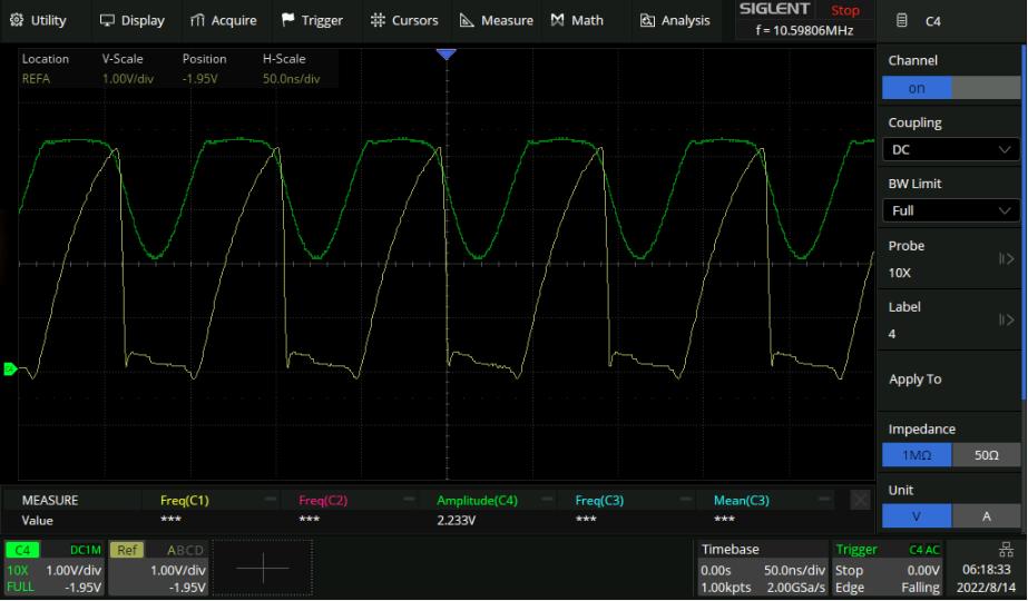
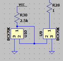
The above are the two buffered outputs with the 1000:1 divider. There is a 43% duty cycle that’s basically independent of LO frequency! I used these values to do the baising:
and one BRF106 can be used to bias two amplifiers no problemo.
Back to the phase detector
Closing the loop on the phase detector makes things get pretty wild:
I haven’t seen that particular pattern of wackery before. Not sure what’s going on. It’s not the popping behavious from before I think.
Boom. Locked.
I noticed before that the bandwidth was only 150KHz. I also noticed that the gain was a fair bit higher than it needed to be. Increasing the 3dB bandwidth to 1MHz by changing R27/C5 to 1kR/150pF:
Increasing R26 only to 1kR changed the gain to ~2. I correctly decided that R25 is not very important.
Here is an image of the thing locked with a 1.4V modulation amplitude:
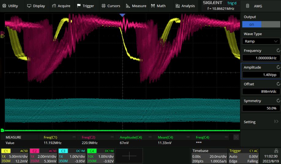
The shape of the modulation is garbage cause of the 1000:1 divider. Here is the input/output shape:
…obviously needs a tad more lowpass on the output there but otherwise hunky dory.