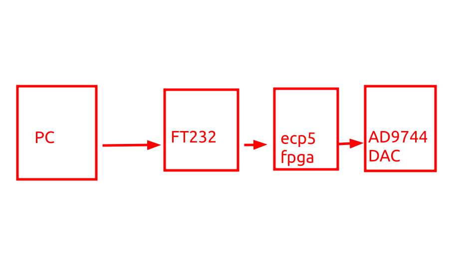
Architecture as it stands
Have not written much here recently as I have been working on the waveform generator PCB, as well as sprucing up the code to drive it. The architecture of the system now looks like this:
The main effort within the code went towards expanding the bit width of the bus, adding actual test coverage, and making a python API that is reasonable. Now, to send a signal out you just have to do this:
import libawg
awg = libawg.awg(transmit_size=int(0))
samples = np.sin(np.linspace(0, 2 * np.pi, 10000)) * 0.5 + 0.5
result = awg.send(samples, trigger_mode=vc.TRIGGER_MODE_NONE)
As opposed to the absolute travesty that existed before.
Testing
The ability for iverilog to actually test things appears to be zero. In addition to that, verilog continues to astound me with its willingness to compile code that just makes no sense. Do you think that this C program should compile?
int func1(int arg1, int arg2) {
	return arg + arg2;
}
int func2() {
	return func1(3);
}
No. of course not. That would be bananas. And yes, you can synthesis verilog modules where half the wires are missing. What’s up with that? Absolutely insane thinking. Verilog will at least print a warning (that I haven’t been able to turn into an error), but the warning is buried in 1000 lines of random debugging trash to guarantee you’ll miss it.
So what I did was just ask claude to write me a program that parses the output looking for warnings and dies if it finds any. That way I don’t waste my time debugging something that should never have compiled in the first place. It looks like this:
#!/bin/bash
# Run the test and highlight errors and warnings in red/yellow while preserving all output
make sim 2>&1 | tee /tmp/test_output | while IFS= read -r line; do
    if [[ $line == *ERROR* ]]; then
        echo -e "\e[31m$line\e[0m"  # Red for errors
    elif [[ $line == *warning* ]]; then
        echo -e "\e[33m$line\e[0m"  # Yellow for warnings
    else
        echo "$line"
    fi
done

echo -e "\n=== Test Summary ===\n"

# Check for errors or warnings in the saved output
if grep -iq 'warning' /tmp/test_output; then
	echo -e "\e[33mWarnings found during synthesis ❌\e[0m"
    rm /tmp/test_output
    exit 1
else
    echo -e "\e[32mSynthesised without warnings. ✓\e[0m"
    rm /tmp/test_output
    exit 0
fi
Test data generation
I have code on the host python side that is responsible for taking waveform generator samples and then packing them onto the wire. Said code is also of course tested to work. But, I want to use samples in the wire format for my unit tests. Previously I did this with an actual verilog module that created the required data: (abbreviated):
module generate_alternating_test_vector;
    parameter BW = 8;
    parameter PAYLOAD_LEN = 0;  // Must provide

    // Actual command stream being sent to the fpga.
    reg [BW - 1:0] byte_stream [0:PAYLOAD_LEN - 1];
    // Ground truth of the awg samples intended to be sent.
    reg [BW - 1:0] awg_stream [0:PAYLOAD_LEN - 1];

    integer bit_idx;
    integer data_byte_idx;
    reg [BW - 1:0] awg_byte_idx;

    initial begin
        for (awg_byte_idx = 0; awg_byte_idx < PAYLOAD_LEN; awg_byte_idx = awg_byte_idx + 1) begin
            awg_stream[awg_byte_idx] = (awg_byte_idx % 2 == 0) ? 16'hFFFF : 16'h0000;
        end

        byte_stream[0] = `TRIGGER_MODE_NONE | `CMD_MASK;

        for (bit_idx = 0; bit_idx < PAYLOAD_LEN * (BW - 1); bit_idx = bit_idx + 1) begin
            data_byte_idx = bit_idx / (BW - 1);
            byte_stream[1 + data_byte_idx][BW - 1] = 0;
            byte_stream[1 + data_byte_idx][(BW - 2) - bit_idx % (BW - 1)] = awg_stream[bit_idx / BW][BW - 1 - bit_idx % BW];
        end

        byte_stream[PAYLOAD_LEN - 1] = `RESET_TRANSMISSION | `CMD_MASK;
    end
endmodule
But then this didn’t work when I had to expand the bit width of my DAC output from 8 to 14. So instead, I now do this 😈:
def emit_verilog_module(samples: np.ndarray, trigger_mode: int):
    bytes_out = wire_format.samples_to_wire_format(samples, trigger_mode)
    module = f"""

module test_vector_{vc.const_to_string(trigger_mode)} # (
   parameter NUM_TEST_SAMPLES = {len(samples)},
   parameter NUM_TEST_BYTES = {len(bytes_out)}
) ();
   reg[15:0] sample_stream[0:{len(samples)-1}];

   reg[7:0] byte_stream[0:{len(bytes_out)-1}];
   initial begin

"""
    for i, byte in enumerate(bytes_out):
        module += f"       byte_stream[{i:02d}] = 8'b{byte:08b};\n"
    for i, sample in enumerate(samples):
        module += f"       sample_stream[{i:02d}] = 16'b{sample:016b};\n"

    suffix = """
    end
endmodule

"""
    module += suffix
    return module

def gen_test_data():
    samples = (np.arange(1, 6) % 2).astype(np.uint16)
    samples = samples * 0xFFFF
    assert samples.dtype == np.uint16
    filename = "../rtl/awg/test_data.gen.v"
    test_none = emit_verilog_module(samples, vc.TRIGGER_MODE_NONE)

    samples = np.array([0xF00F, 0x0FF0]* 3, dtype=np.uint16)
    test_edge = emit_verilog_module(samples, vc.TRIGGER_MODE_EDGE)
    test_data = """
`ifndef TEST_VECTOR_V
`define TEST_VECTOR_V

// DO NOT MODIFY: Generated from gen_test_data.py

`default_nettype none
`timescale 1ns/1ps

""" + test_none + test_edge + """
`endif // TEST_VECTOR_V
"""

    print(test_data)
    with open(filename, "w") as f:
        f.write(test_data)
And stick this in my Makefile:
.PHONY: sim
TESTBENCH_DEFINE = -DTESTBENCH
sim: top_sans_ftdi_tb.vcd
top_sans_ftdi_tb.vcd: $(SIM_SRC)
	python ../../python/gen_test_data.py  # Regenerate test data
	iverilog -Wall -o top_sans_ftdi_tb.vvp $(TESTBENCH_DEFINE) $(SIM_SRC) test_data.gen.v
	vvp top_sans_ftdi_tb.vvp
I never claimed this project would use good software engineering practices, you know.
AD9744
I whipped up a quick board for the AD9744, so now my test setup looks like this:
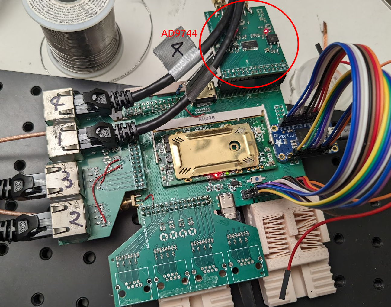
The output isn’t buffered or anything like that, and the DAC is a current output DAC. So I just 50 ohm terminate it in my scope and call it a day. Despite the data sheet only specifying the analog performance out to 10MHz, it says that on the digital side it can be updated at 100MHz+, and indeed I see only a couple ns settling time for it! So I don’t know what they’re talking about there. Maybe I can even use this for my next 100MHz revision of the AWG.
14 bits
The DAC is 14 bits. Having an actual 14 bit width number being sent over on the host PC side would be a pain, so what I’ve decided to do instead is use the two remaining bits and dedicate them to digital outputs. That way you can embed some digital controls in the output stream, which is nice.
So from the point of view of everything, even most of the verilog, it’s a 16 bit DAC. It’s just that I strip out the bottom 14 bits to actually go to the DAC and send the top two to digital output lines instead.
PCB
Now that I have all the main ingredients, it’s time to combine them onto one big PCB. This is my first fpga project, so I went and had a look at the orange crab and ecp5-mini projects. They also have a 1BitSquared discord in which the authors are very helpful. Anyway the PCB is nothing special, and looks like this:
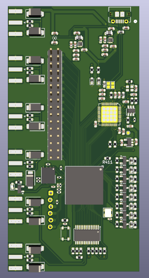
Although it only took 4 layers to route it, it uses the JLCPCB 6 layer fab process as it has via-in-pad, which made routing out the BGA a breeze. I went to the BGA-256 package as it has a larger pitch between balls as the 381 and others.
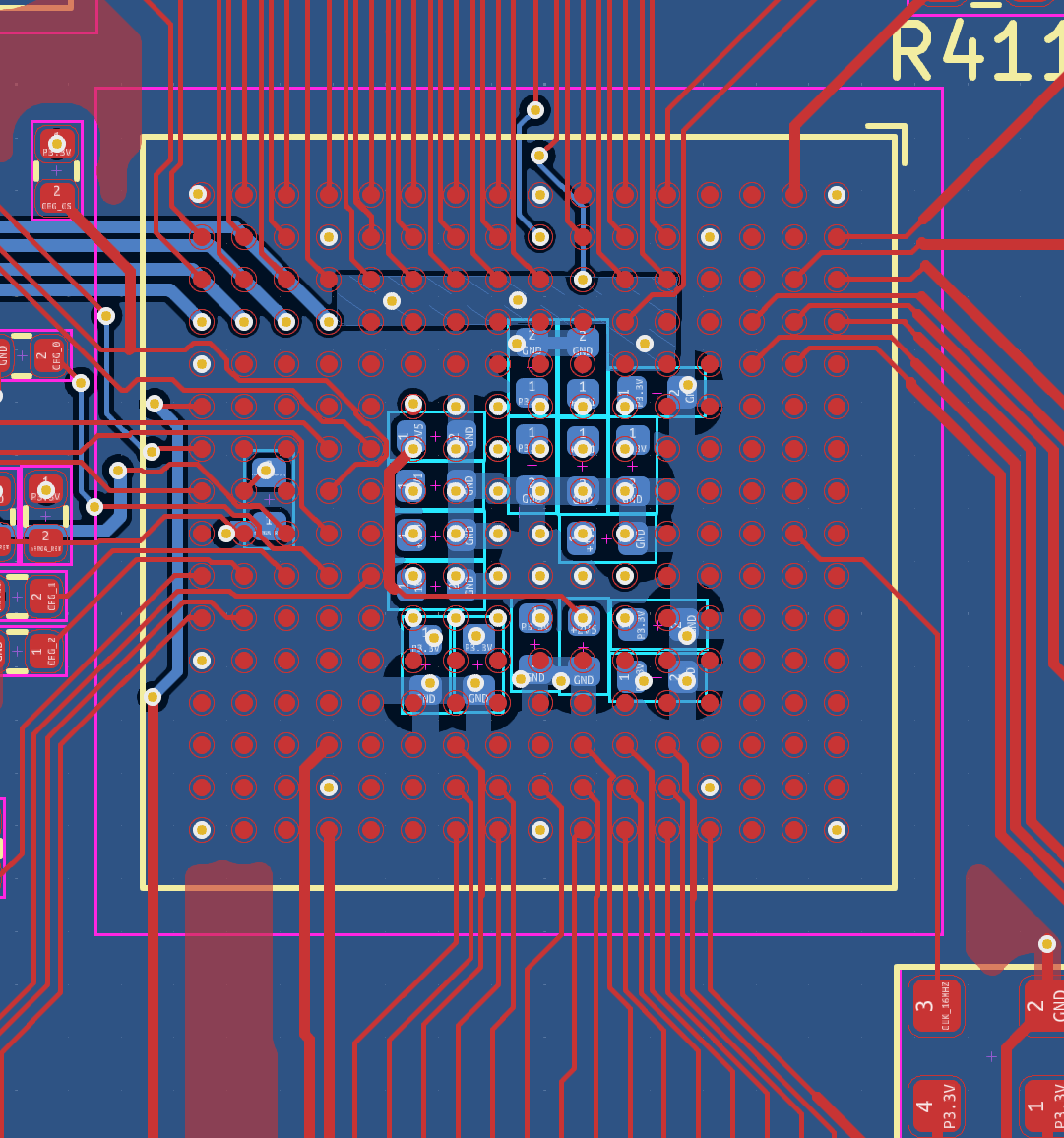
BGA fanout:
Even so, all-up with assembly for two of the boards it cost $200USD to deliver to my house. Ouch.