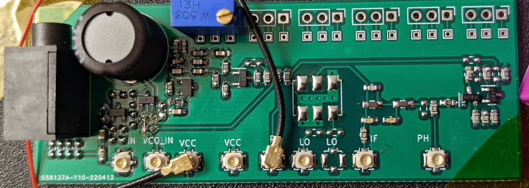
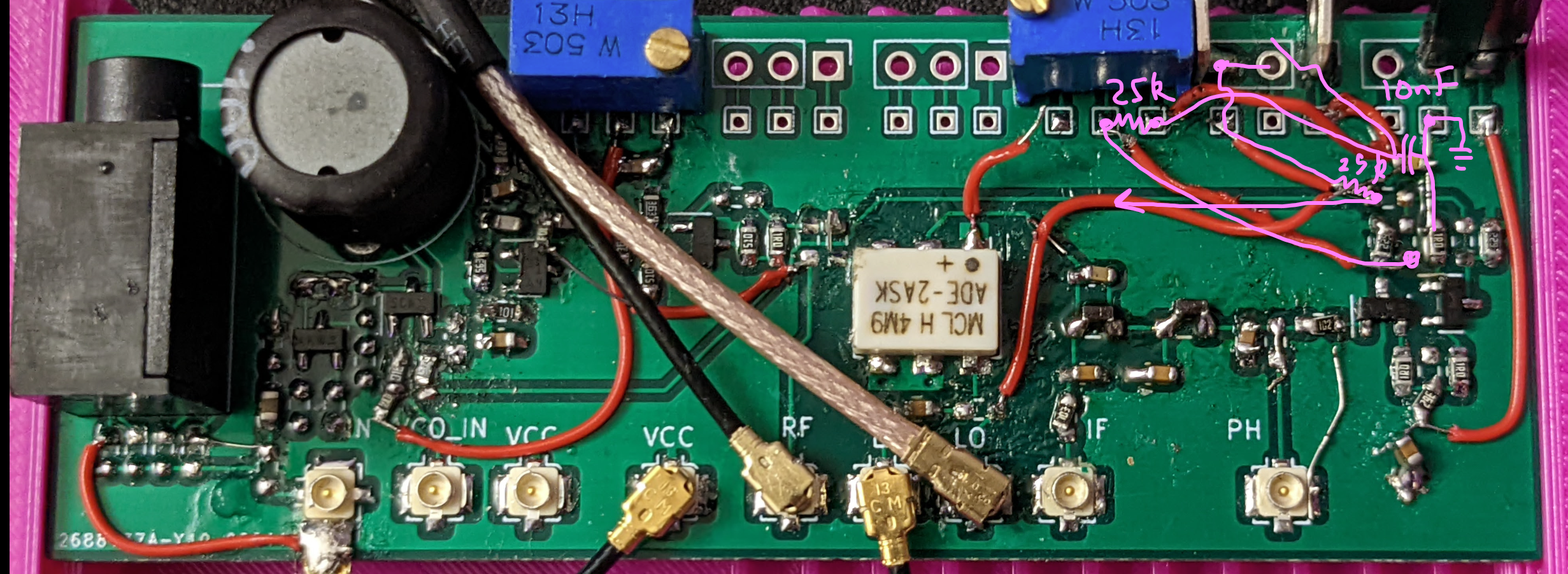
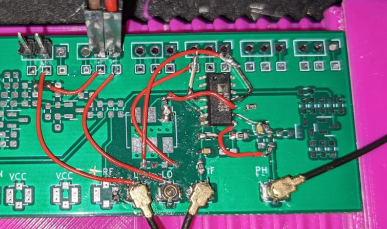
Board
Populated most of the things:
Might be a bit inconvenient to probe. Output does not oscillate, of course.
Debugging
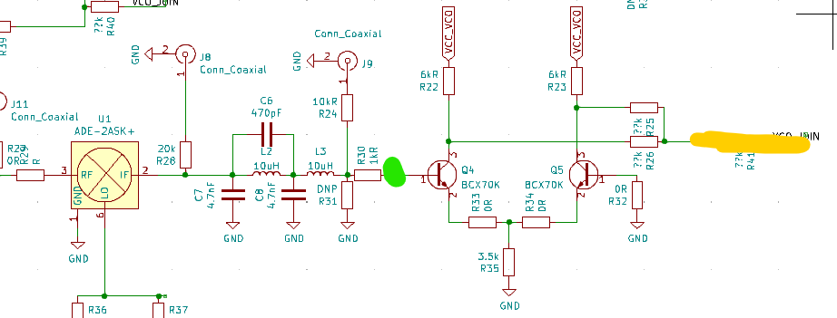
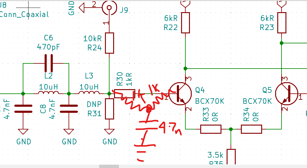
Relevant section of the schematic:
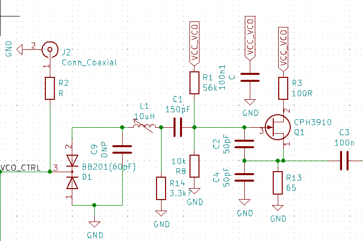
First things first: check the bias on the transistor. I think R13 is way too low by the way. after desoldering the working oscillator it’s 131R
Initial observations
Q1 Vg = 1.131, Vs=1.396 ⇒ Vgs = -0.265 So according to datasheet:
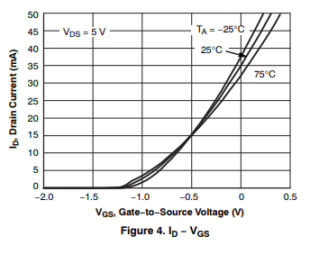
The current should be around 25mA. R3 is 100R and I measured 1.382V ⇒ 13mA. Seems quite low! The quiescent current of the JFET seems roughly similar to the working set so I think it’s most likely the C4/C5 values that are off, and I don’t know what the right ones are. Time to use the VNA!
What’s that capacitor:
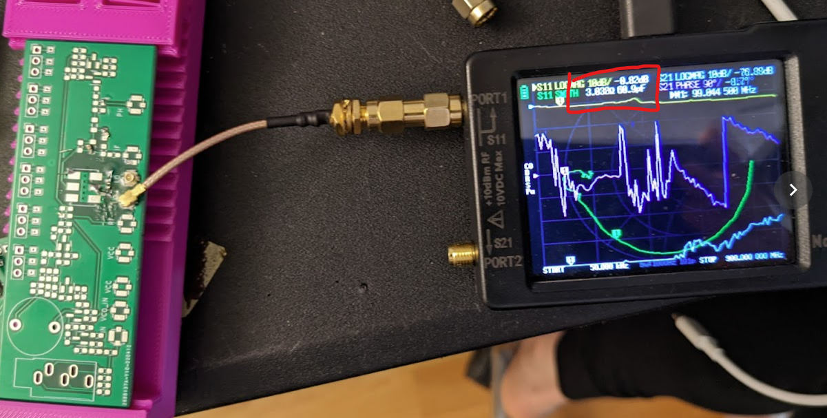
Test setup 1: using the above PCB to easily connect components to the VNA over a UFL connector:
- 56pF is measured at about 61pF
- The cable by itself (even after calibrating) seems to be about 3.4pF. Maybe I need to have a more stable test setup.
- 9.1pF is measured ass 13.6pF. subtracting, that’s 10.4pF. Aliexpress “tolerance” is 5% so that may well be right
- C2 on the above schematic was measured at 105pF
- Adding some flux changed the open circuit capacitance to 3.7pF
- C4 on the above schematic (soldered as two in ||) was 325pF Now to resolder the above values to the new pcb! This gets the oscillator running just fine. Note: decreasing R13 to 65R stops the oscillation.
First mixing
Here is an image of the phase output, and then the output of the diff amp that amplifies that phase:

All of this is looking pretty spiffy so far.
Measurements of inductor
The big coil inductor works but the small 0603 inductor does not. Why?
I think that this measures the inductance:
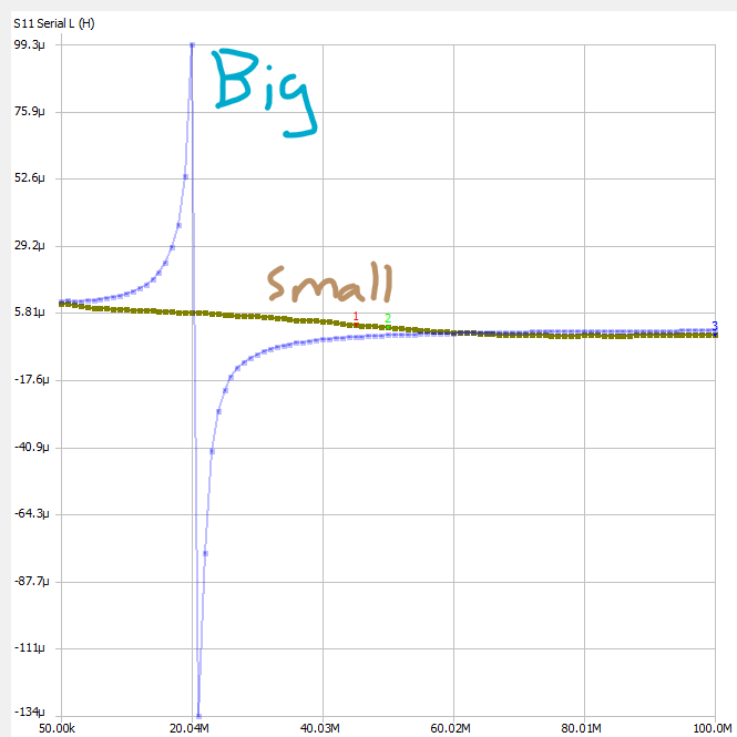
Incomprehensible chart:
It’s unsurprising that the small inductor works better at higher frequencies, but it’s a bit surpriing that it works that well. Both inductors measure about 10uH at 50kHz.
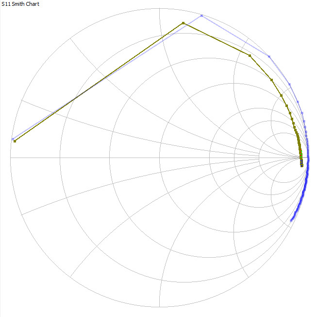
Here’s what it looks like at 50kHz-900MHz:

Allegedly the small inductor (L0603B100KDWFT) is also wire wound so I would have thought it would have the same overall shape as the larger inductor.
Things stop working
The first new asembled board stopped working for some reason. 2.124V across the drain resistor of 100R ⇒ 21mA VDSS. Datasheet says it should be 35mA but there are some resistors in the way. The transitor on the working one is 2.181V, so clearly transistor isn’t busted. Things started working again. I think it’s cause if the VCO is not at a defined voltage then things get wack.
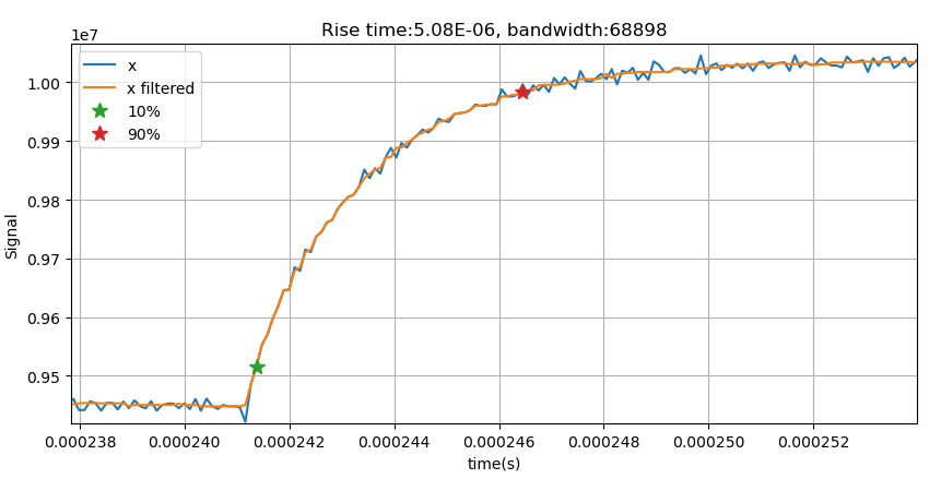
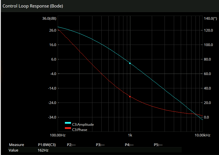
Response time of VCO:
Max F dev: 6.05e5. Min: 2.8e4. ⇒ 90% = 5.47e5. 10% = 8.5e4 t_90: 1.493ms, t_10 = 1.544ms. ⇒ Bandwidth = 0.35/(1.544e-3 - 1.493e-3) = 6.8KHz. This would seem rather too low. That’s with a 50k. Resistor. Should go back to 10.7kOhm 10.7kOhm leads to 68kHz bandwidth:
Slowing things down (dumb version)
As per before we now need to slow down the response of the loop filter to be slower than that of the VCO. I did this like so:
So that should be 30kHz bandwidth.
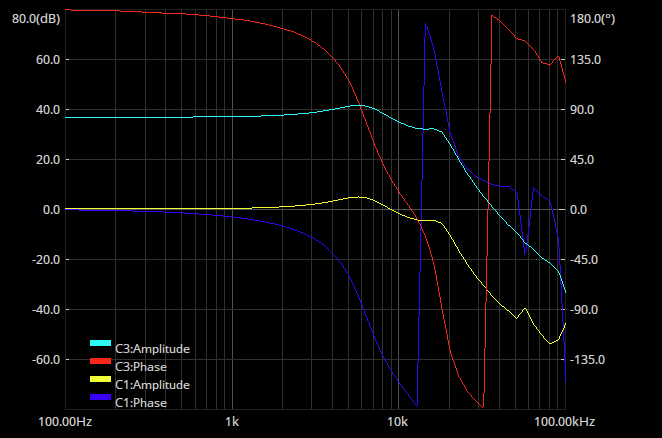
Bandwidth of loop filter
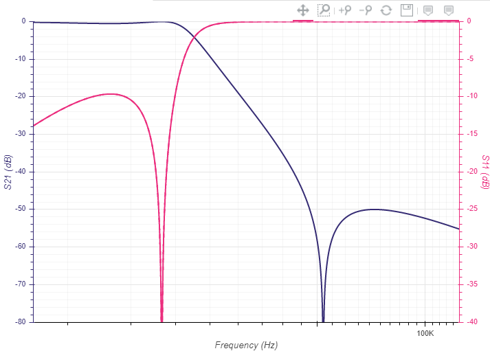
Here is the bandwidth of the loop filter after adding the 30kHz mod:
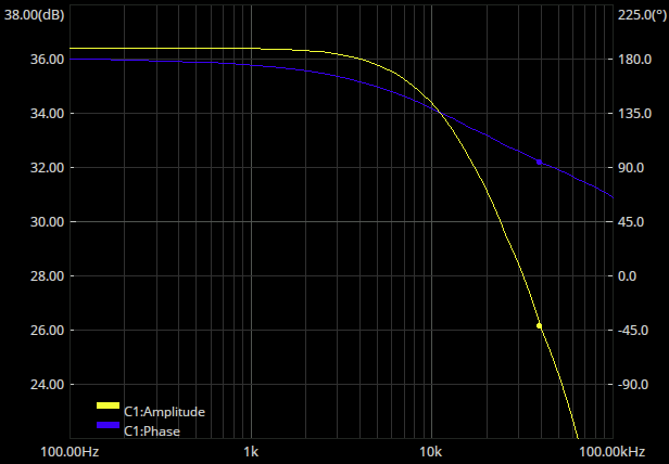
Hit the nail on the head there. You can also see that the diff amp has oodles of gain. But wait! This is the bandwidth of just the passive component of the loop filter
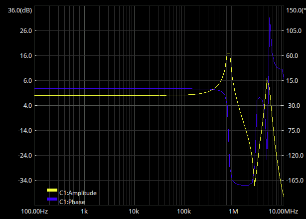
That’s a bit surprising. This completely passive filter has a gain of 13dB? Time to collect my nobel prize for violating thermodynamics.
…Yep. Now that’s what I call resonance! Take note of the y scale.
This is the diff amp by itself:
…I feel like it should have more bandwidth than this. LT spice agrees and says it should be 1MHz. Probing around does not reveal anything noteworthy. It might be worth doing a common emitter amplifier configuration just to check against the spice model.
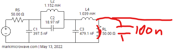
Although the “3dB” point of this system is 30Khz, it still has 20+dB of gain at 60kHz. So to get <<0dB of gain at 60khz I think moving the elliptical loop filter to a much lower bandwidth is in order. The filter tool says this:
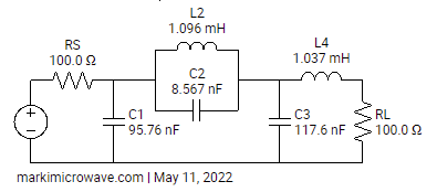
(adjusted the impedance to get 1mH inductor value.) That did not seem to be good enough. This works better:
Where C3 is the passive filter + diff amp and C1 is just the passive filter. The output crosses 0dB gain at about 30kHz and is at ~-10dB at 60kHz so hopefully this will be good enough. If this doesn’t work then reducing the rather large gain of the diff amp would be a good next step.
…This produces utter trash:
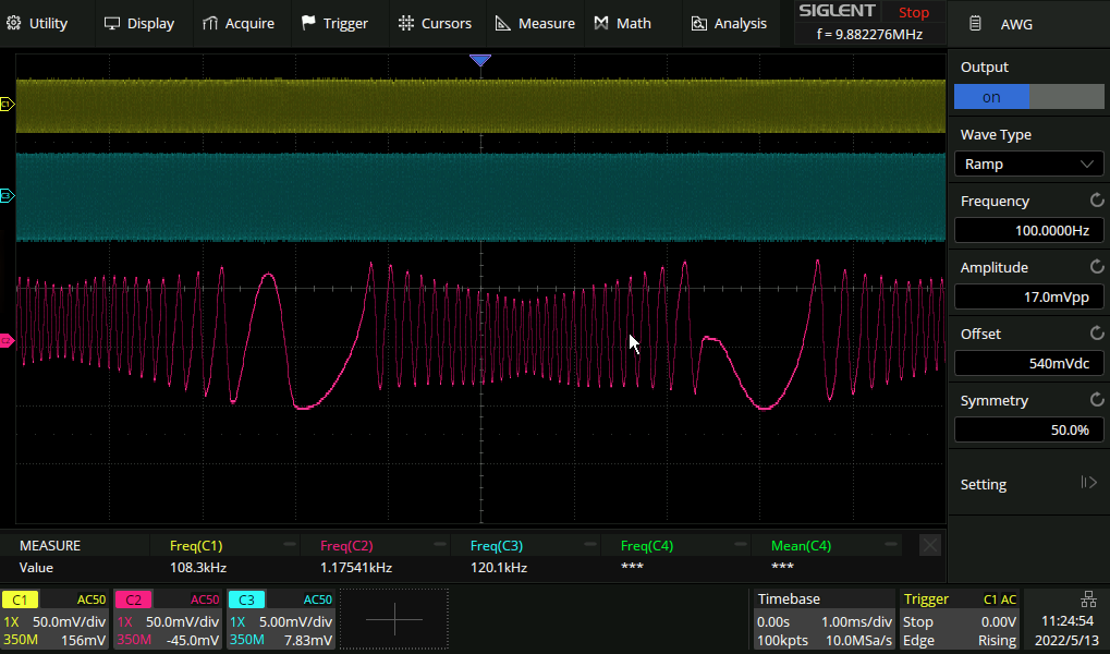
In the above trace Channel 2 is the phase output as a result of sending in a 17mVpp ramp wave in. Changing the offset by 10mV is enough to render the signal borderline unusable and so I take it from that that the control output would also be like 10mV. So I think increasing the bandwidth of the loop filter a whole bunch and going back to a lower gain amp is the way to go.
Quick note: phantom lock
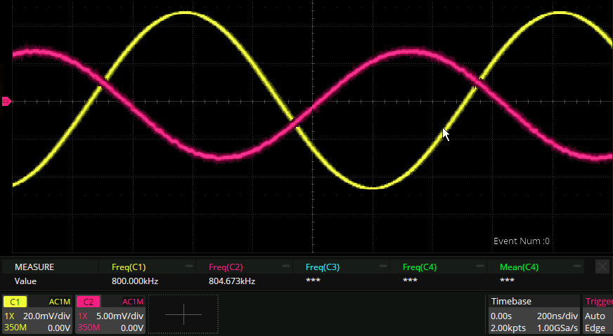
We have a lock:

Situation: control loop switch is open. Channel 1 and two are the RF and LO signal respectively. CH3 is the VCO voltage, about 7.5V. CH4 is VCC (7.97V) V_lo = 1.395V, V_ The circuit is like this:
It’s clearly coupling in through the air somehow, waving a screwdriver around nearby can make it lose the lock. I think the key takeaway here is that the required voltage to lock (7.5Vish) is way higher than makes sense at first glance, it should be like 2V. I suppose given the fact that the control loop is open the actual DC voltage is not important, it’s how it affects whatever dynamic nonsense is being used to close the loop through the aether.
- Disconnecting the output of the diff amp completely still allows the PLL to lock.
- After doing the above the switch (that is connected to the varactor diode but not the output of the diff amp) still prevents the circuit from locking when the switch is closed. This is weak evidence for that long trace running across the board acting as an antenna.
- Desoldering the resistor that attaches to the VCO has no effect, it can still lock. I now presume that the locking is occuring through the mixer somehow. It only happens over a tiny (10’s of mV MAX) voltage range as you would expect.
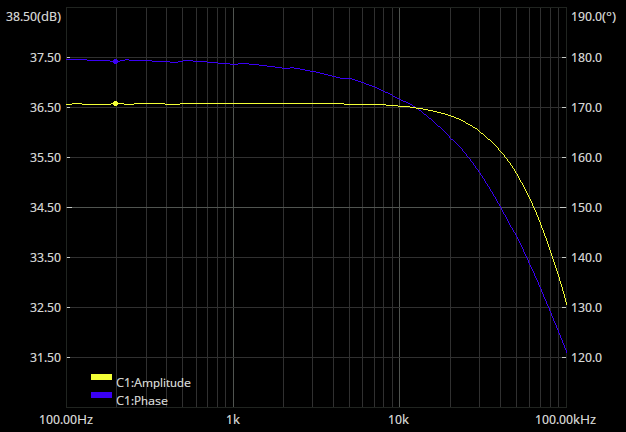
Quick note: phase shift
Here is the output of the loop filter with a nice big capacitor and resitor for lowpassing. As you can see this has apalling phase performance. So I think going to the example filter in “Introduction to radiofrequency design” is a good idea as a sanity check.
Note that the filter in the textbook is designed assuming a 1000x divider on the output of the VCO before it goes into the mixer.
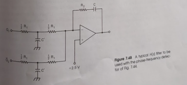
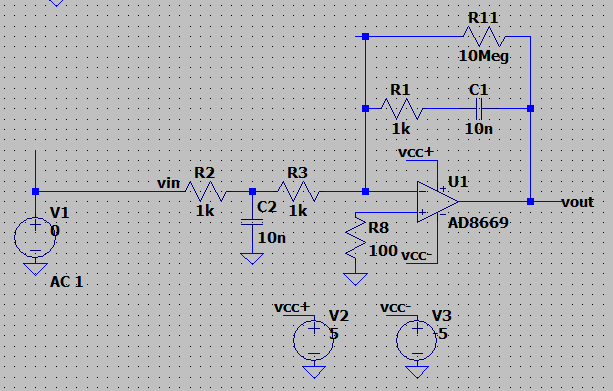
The circuit has been built:
Note that a 10Meg resistor was added across the cap for the required DC path, and a 100R resistsor was added as an output load in an attempt to stabilise the DC output point of the amplifier, which varies by many V depending on cable positioning etc.
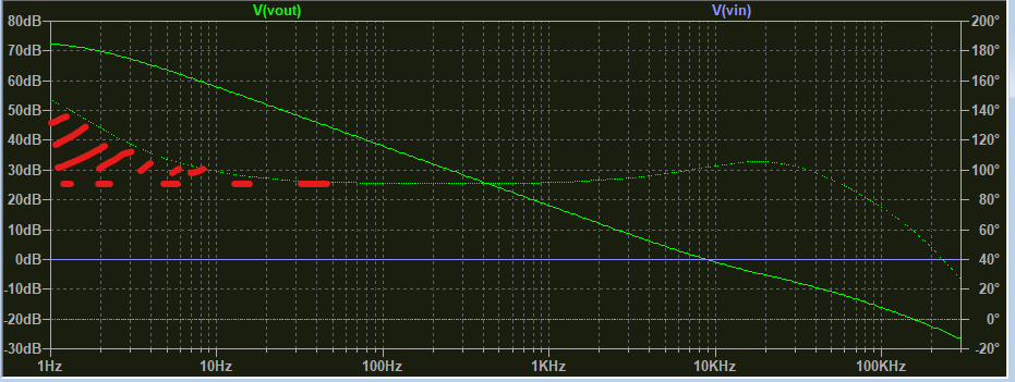
The red shaded area above is due to the 10 Meg resistor. Here is the bode plot:

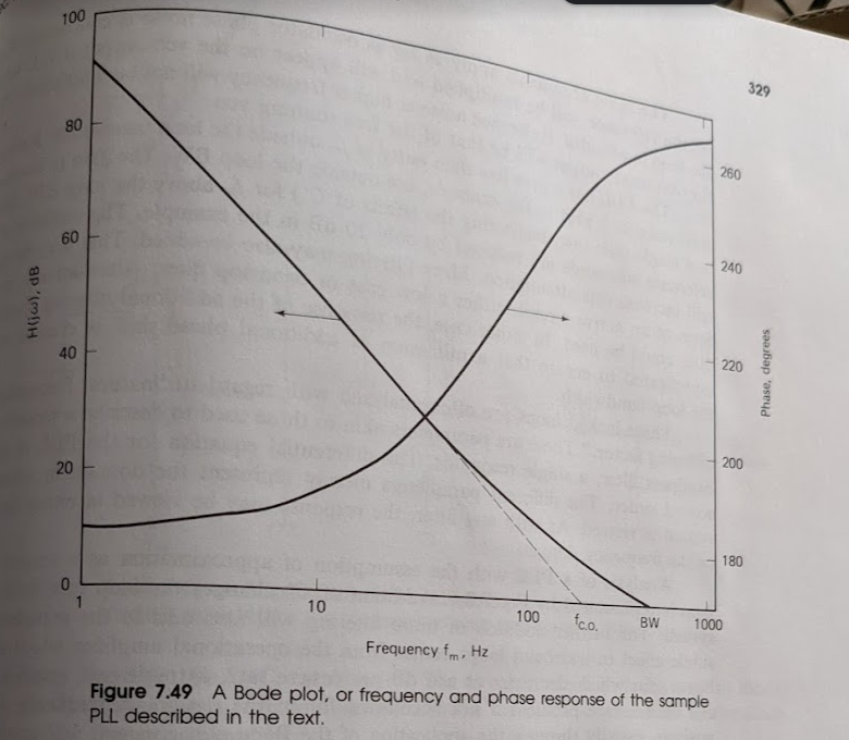
Looks vaguely the same, exept that the phase shift component from the 10Meg resistor is missing. Suspicious… I’m also a bit worried that the phase shift goes up by a fair bit before the amplifier crosses zero gain. The textbook says it should look like this (I think):
The main troubling thing here is that the phase shift in the book is 180deg (negative feedback) but the sims and real life show 90 degrees. What gives?
Results
Needless to say, this does not work. It seems to get into the state where the F(VCO) > F(RF), and then you can adjust the RF frequency up and down with the VCO frequency sitting at some extra frequency above that, say +300kHz. I really think this must have something to do with the phase shift still for some reason. The whole point of this filter was that it was supposed to be out-of-the box working and given the phase shift is wildly different from what the author thinks it should be, it’s time to move on I think.