Off the bat
It seems that straight off the bat the oscillator oscillates. One small problem though, it only does that at a very specific range of temperatures. Here is the circuit deciding whether or not it is at the right temperature:
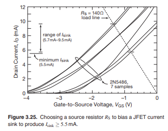
 I recall seeing in the art of electronics that JFETs have a large variability in their gain and Vgs and whatnot from sample to sample. So it’s a good guess that’s what’s going on here. From the third edition:
Going off the general principle that more bias current is good for everything except power consumption, let’s try increasing it.
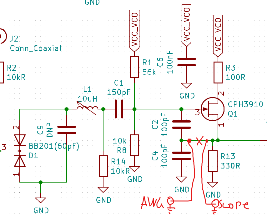
As a reminder, here is the circuit:
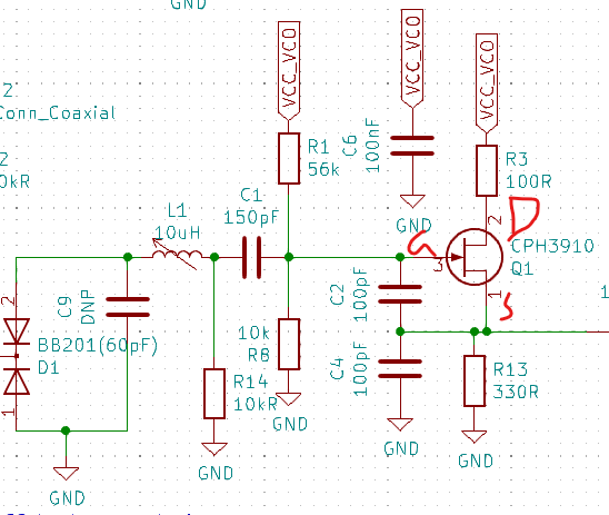 Since is set by and is set by the R1/R8 divider we can say that:
Note that in practice is a negative voltage.
Since is set by and is set by the R1/R8 divider we can say that:
Note that in practice is a negative voltage.
Sanity check
At this point it occurs to me to measure the drain current and look at where it sits on the characteristic curves in the datasheet…
Vg is 716mV. Vs is 1.40V. Vd is 4.18V. So Id is (4.6 - 4.18) / 100 = 4.2mA, or 1.4 / 330 = 4.2mA.
⇒ is -0.684V, and we sit here on the operating curves:
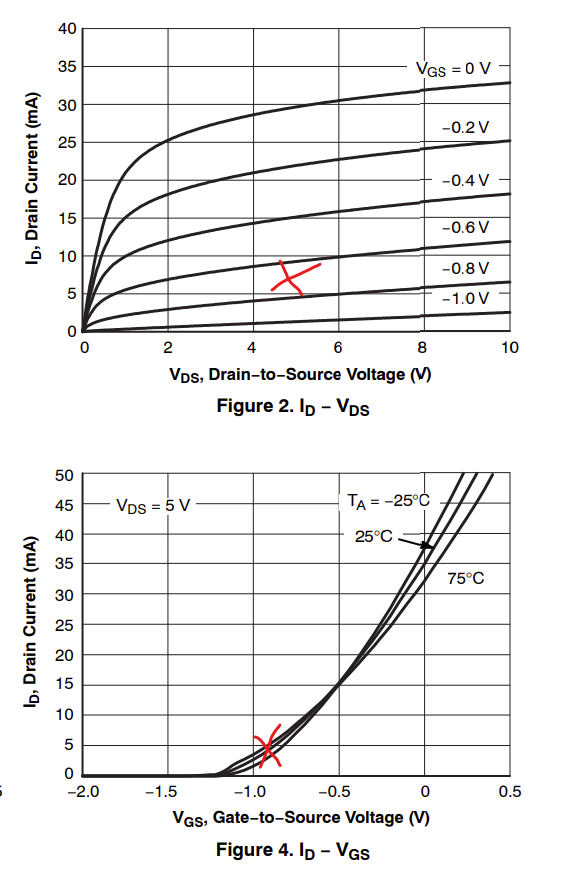 Seems about right to me.
Note: when I adjust vcc up to 5.0V things become unstable in the same way as described in the beginning . Good way to check for better stability later. Adjusting the oscillator frequency to 10.0MHz from 10.2 also makes it more stable. This required a varactor voltage of 1.18V.
Circuit B
I assembled two:
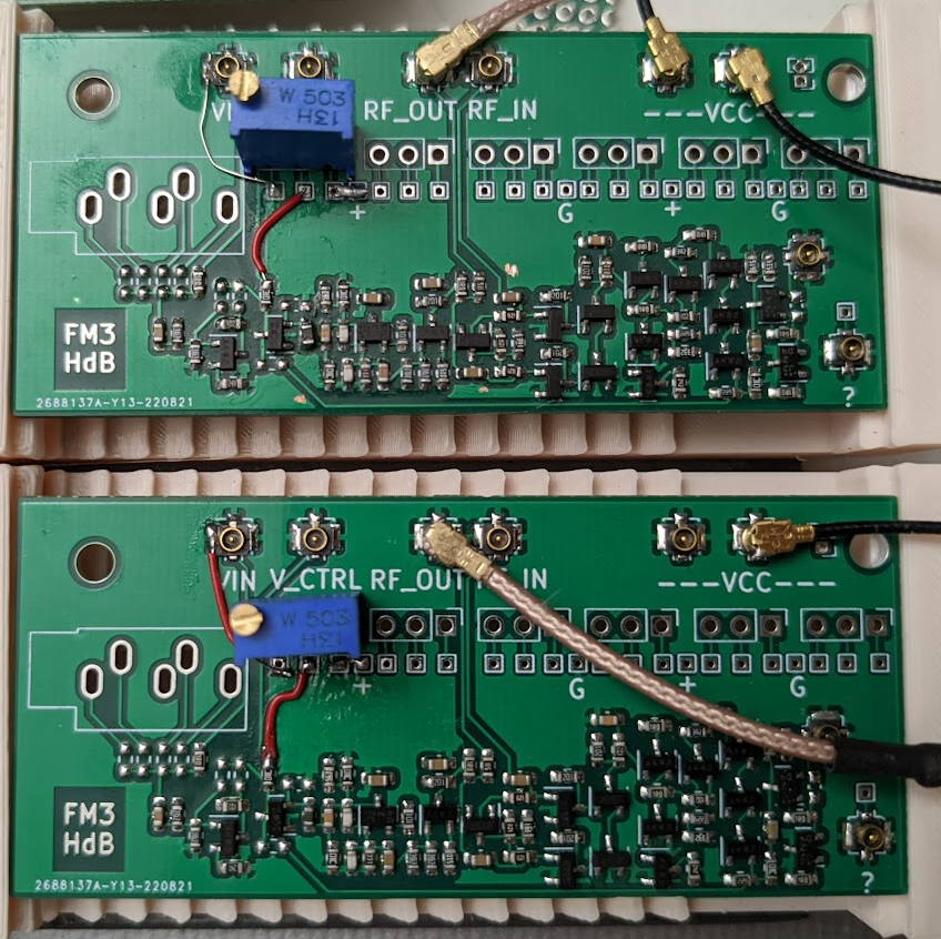 Of these boards (Henceforth known from the top down as A and B) and the bottom one does not oscillate at all. We shall measure the same JFET parameters. I think maybe I am being bitten here over and over again by the JFET variability and I need a proper current source on the source of the JFET, taking the output of the oscillator from the drain. I don’t know if this would actually work though.
Vs = 1.36V, Vg = 0.705V, basically the exact same. y u no oscillate?
I desoldered the next stage of gain from both A and B to try and find differences. This just caused A to stop oscillating as well. I really gotta figure out the whole stability thing here so I can solve this once and for all.
Of these boards (Henceforth known from the top down as A and B) and the bottom one does not oscillate at all. We shall measure the same JFET parameters. I think maybe I am being bitten here over and over again by the JFET variability and I need a proper current source on the source of the JFET, taking the output of the oscillator from the drain. I don’t know if this would actually work though.
Vs = 1.36V, Vg = 0.705V, basically the exact same. y u no oscillate?
I desoldered the next stage of gain from both A and B to try and find differences. This just caused A to stop oscillating as well. I really gotta figure out the whole stability thing here so I can solve this once and for all.
Colpitts oscillator phase margin.
I should figure out this phase margin thing. I don’t really know how to measure it though, that’s the main problem. Some textbook called “Foundations of oscillator circuit design” has this to say on the topic:
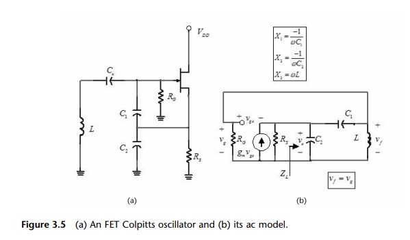
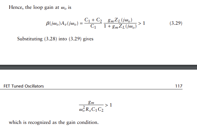 I believe is the gain of the transistor. is fixed (10Mhz) and I don’t particularly want to decrease because that would mean I needed more collector current for the same output swing.
I also don’t find this model intuitive. The way I have thought about things before is that C1/C2 are a feedaback divider, and so increasing C2 would put more of the RF output to ground, lessening the phase margin. But here they are saying that C1 and C2 affect the output of the circuit in exactly the same way, which I find very suspicious.
The textbook overall seems to be of the rather common “giant pile of useless algebra” variety, failing to mention, for example, how one might measure the phase margin of a circuit.
I believe is the gain of the transistor. is fixed (10Mhz) and I don’t particularly want to decrease because that would mean I needed more collector current for the same output swing.
I also don’t find this model intuitive. The way I have thought about things before is that C1/C2 are a feedaback divider, and so increasing C2 would put more of the RF output to ground, lessening the phase margin. But here they are saying that C1 and C2 affect the output of the circuit in exactly the same way, which I find very suspicious.
The textbook overall seems to be of the rather common “giant pile of useless algebra” variety, failing to mention, for example, how one might measure the phase margin of a circuit.
Split the loop
One thing that I have noticed consistently comes up in textbooks when discussing phase margin and stability etc for PLL’s and oscillators is the concept of “splitting the loop” where the circuit is split at some point and it’s verified that the output of the circuit is both higher and in phase on one side of the split than the other.
Seems like a good idea to try here. I think in this case it would look like this:
Results
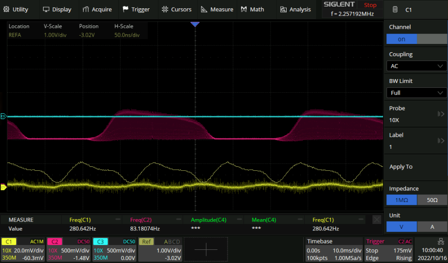
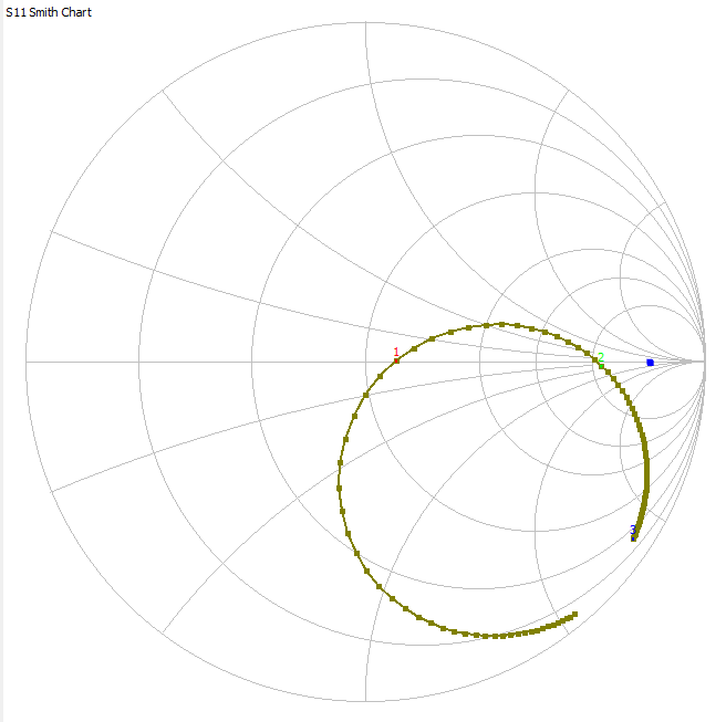
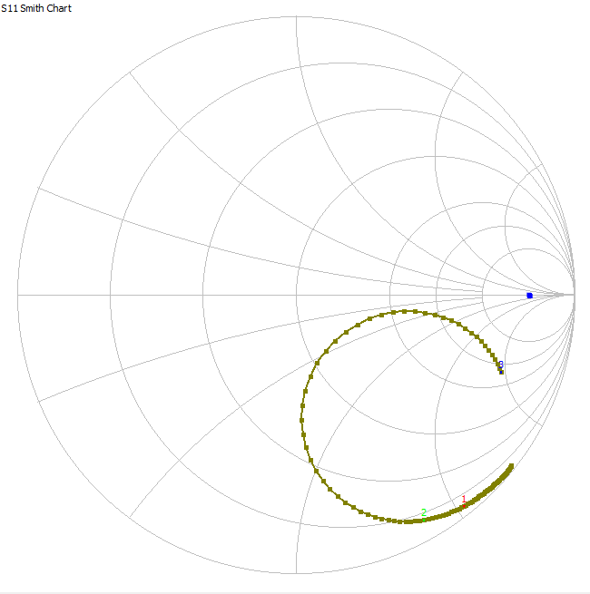
I used the nanovna to get these results. I put a 500R resistor on the output though so as not to load down the circuit. Here they are in a smith chart that I don’t understand but seems to show something important (maybe my circuit is the same as a capacitor?):
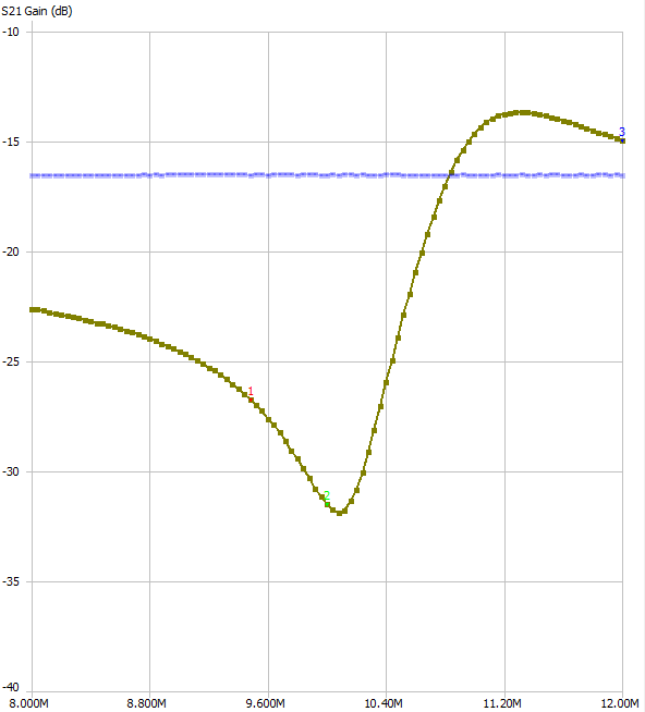
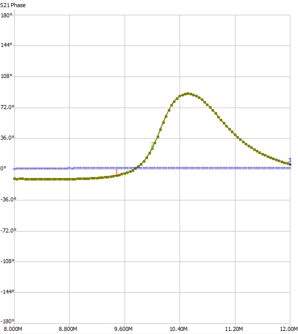
 And here are the the more intuitive S21 gain and phase plots:
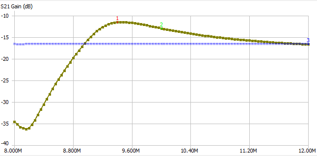
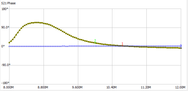
The reference trace here is the attenuation in the system. So in the gain plot everywhere the gain is above the reference line it is above 0dB gain.
One thing that struck me was the S11 return loss:
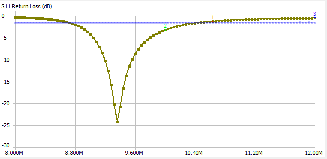 I think this means that the output of the amplifier sees a dead short basically at 9.34MHz. That doesn’t sound great.
Regardless it looks like the max gain is +5dB at 9.48MHz, and overall I think the plots more or less make sense. The gain is >0dB (but not by much) and the phase is close to 0 degrees (but varies wildly).
Next I think I will take another measurement with the varactor at a higher voltage. In the above measurements it is at 1.19V. Here it is at 4V:
I think this means that the output of the amplifier sees a dead short basically at 9.34MHz. That doesn’t sound great.
Regardless it looks like the max gain is +5dB at 9.48MHz, and overall I think the plots more or less make sense. The gain is >0dB (but not by much) and the phase is close to 0 degrees (but varies wildly).
Next I think I will take another measurement with the varactor at a higher voltage. In the above measurements it is at 1.19V. Here it is at 4V:
 As expected things have shifted to a higher frequency. The peak gain is only like 3dB now though.
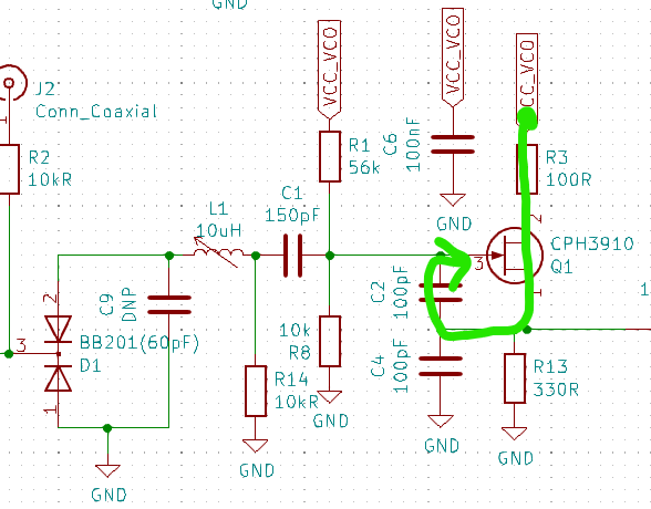
I did some LT spice simulations and from looking at that I came to the conclusion that reducting the drain resistor is what is needed here. This is because the impedance applied to the gate of the JFET is the sum of the impedance of the drain resistor and the resistor between the source and the gate (R3 + C2):
 Which just like everything else in life makes total sense in retrospect.
LT spice confirms that this should increase the “open loop” gain, let’s take a look irl by changing R3 to 10R.
…And that makes practically no difference. I guess my assumption that the CPH3910 itself was low impedance compared to 100R was false.
After consulting the “High Frequency VCO Design and Schematics” page it seems that increasing the coupling between the LC network D1/L1 and the transistor by increasing C1 can also help. This seems to work OK, the gain increased to a peak of -11.7dB. I think perhaps that increasing C1 to the point where it is very low impedance increases the sensitivity of the circuit to the absolute values of C2 and C4. 150pF is 106R at 10MHz and 8.5nF is 1.5R.
I connected the ends together and it oscillates pretty stably though. The amplitude drops considerably from the heat gun but it still oscillates so that’s OK I think. Sensitivity to vcc is also down so I shall call it a day and change the value permanently.
Which just like everything else in life makes total sense in retrospect.
LT spice confirms that this should increase the “open loop” gain, let’s take a look irl by changing R3 to 10R.
…And that makes practically no difference. I guess my assumption that the CPH3910 itself was low impedance compared to 100R was false.
After consulting the “High Frequency VCO Design and Schematics” page it seems that increasing the coupling between the LC network D1/L1 and the transistor by increasing C1 can also help. This seems to work OK, the gain increased to a peak of -11.7dB. I think perhaps that increasing C1 to the point where it is very low impedance increases the sensitivity of the circuit to the absolute values of C2 and C4. 150pF is 106R at 10MHz and 8.5nF is 1.5R.
I connected the ends together and it oscillates pretty stably though. The amplitude drops considerably from the heat gun but it still oscillates so that’s OK I think. Sensitivity to vcc is also down so I shall call it a day and change the value permanently.
Circuit B
The day was not called. Circuit B was oscillating unreliably. Changed R3 to 10R (probably not important) and C4 to 200pF, then replicated changes on circuit A. Crossed fingers that’s enough