Idea
Resin printers are nothing but and LCD screen with a UV printer behind it. So why not use the LCD screen to expose some PCB’s? Some other people have tried this already so it isn’t new, but it would be pretty handy to be able to get a new pcb in <1hr.
Implementation
Workflow
There are a few tutorials on the internet on how to do this, but they all involve tedious manual tasks like exporting to blender etc etc. I am pretty sure that the file format that the printer itself accepts is a bunch of images, and a gerber file is basically an image, so why can’t I go directly? I found A great guide on the internet written in rust with good documentation (apparently this person is the same person that founded loon) and indeed, this is what the file format is. My code to convert the svg output from kicad to the cbddlp file is here. I bought some presensitized PCB panels from amazon here.
Chemicals
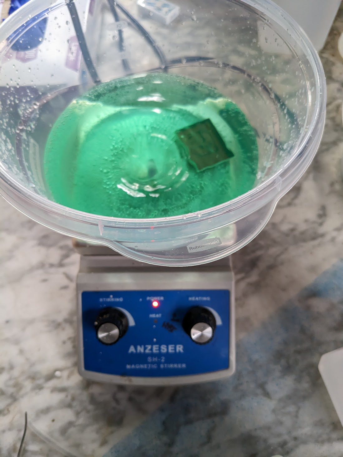
The basic process was expose→NaOH wash→HCl+H2O2 wash.
It took quite a few tries to dial in the process. In particular the exposure time and NaOH concentration took a while to dial in. I ended up putting in half spoonfuls of NaOH to gradually increase the concentration (and I think it still could be a little higher) and so unfortunately I don’t have a proper number. But in the end I got good results. Here is an image of the washing:
 And an image of the etched results:
| Before removing photoresist | The final PCB |
|---|---|
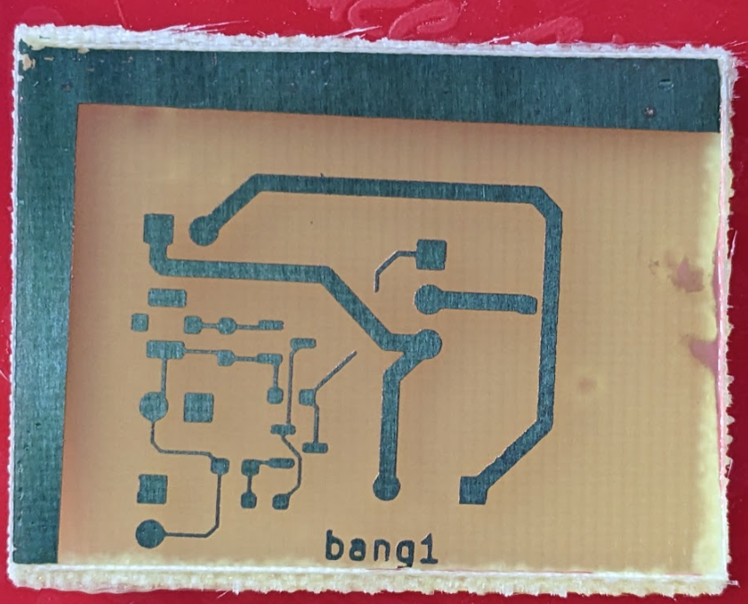 | 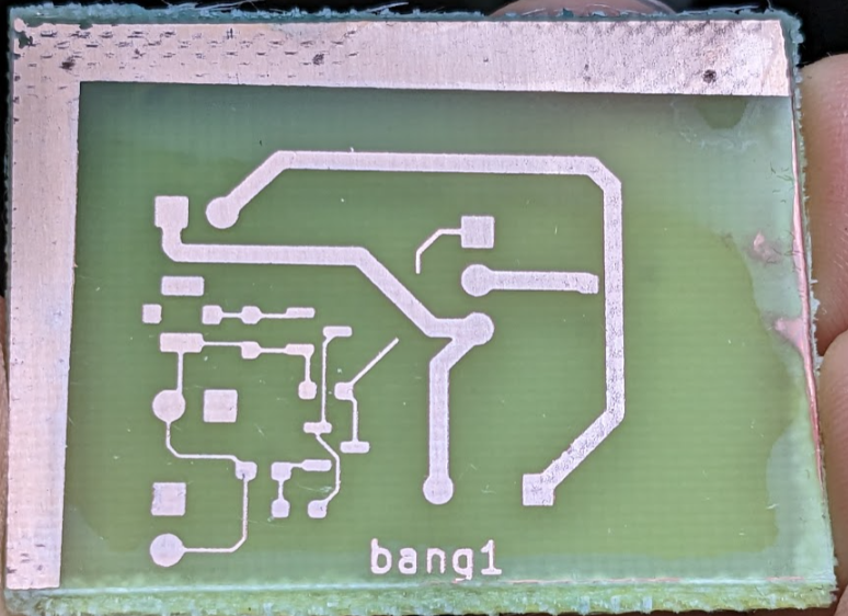 |
Zooming in, let’s take a look at the resolution vs what the printer tried to put out:
| LCD printer image | The final PCB |
|---|---|
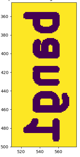 | 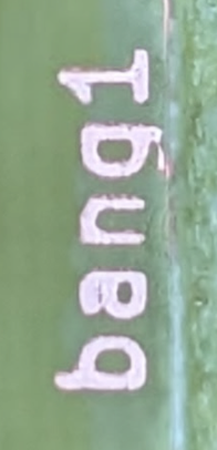 |
| You can just barely see here that the gap at the top of the “a” here is 1 pixel wide, and there is just barely a gap at the top of the a in the printed product. That makes it basically pixel perfect! | |
| The assembled PCB: | |
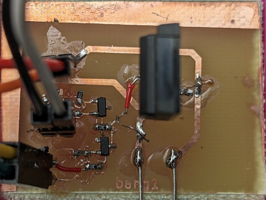 | |
| Success! |