I bought an Agilent 6675A power supply for $40. 110V 18A supply, tremendous.
I plugged it in, set the voltage to 10V. Got 10V, nice. I changed the voltage to 110V and then got this:
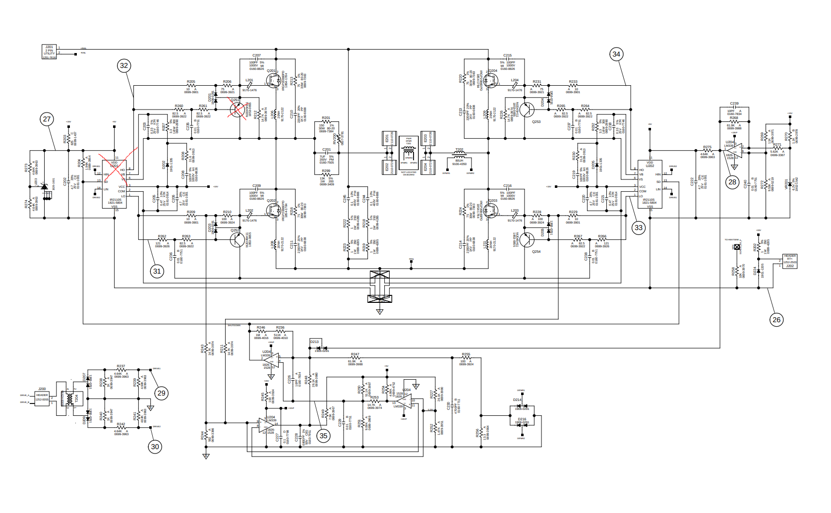
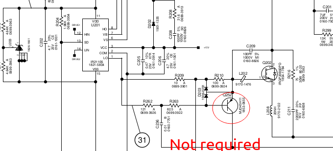
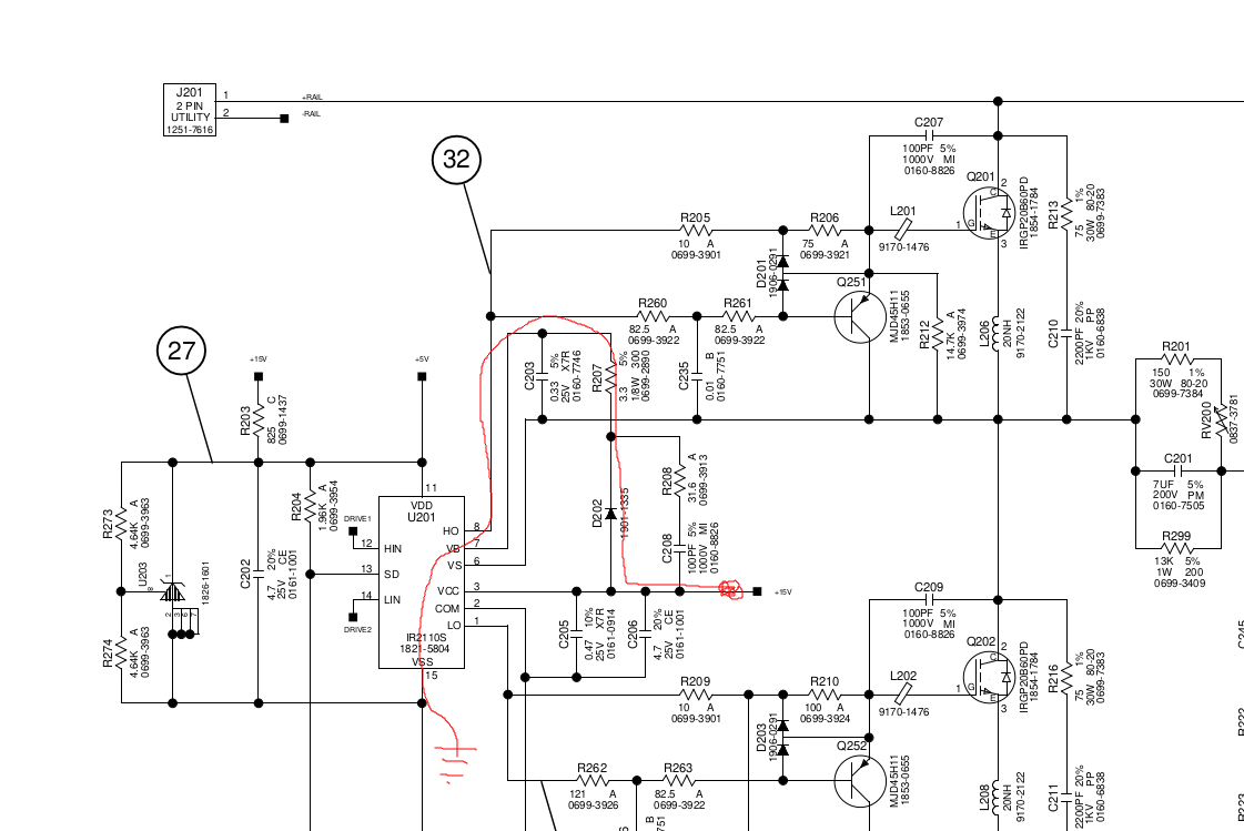
…not so nice. This is the schematic of the above board with what I think blew up crossed out:
…so that’s not great. I purchased a replacement MOSFET driver and a not-quite-replacement npn transistor (TIP42C), then reconnected everything and turned it back on. It turns on and I can set the voltage and current, but the front panel says ‘Unr’ which according to the manual means “unregulated”. Further investigation revealed that the input 240V 20A fuse had blown, so I replaced it with some 0.2mm copper wire, which apparently has a fusing current of like 6A.
After turning on the supply it seemed happier. I changed the voltage to 6V and the power supply said it was in constant voltage mode instead of unregulated mode, nice! Then I turned around to grab the multimeter and the fuse wire I put in absolutely detonated with a loud bang. Not a pop. A bang. This is what the surrounding area looked like afterwards:
…That is a little unnerving. I quickly got out the thermal camera after it went pop to try and catch something red handed, but no luck. Rather than put a piece of wire back and try it all again, I instead went back to the FET board above looking for trouble. This time the pnp Q252 driving the low side FET died. Oh and by the way, the schematic is not the schematic for the board that I have. It’s for a later revision of the board that uses MOSFET’s rather than IGBT’s. Taking the pnp transistor out I see it has failed short.
…Looking at the datasheet for the replacement transistor I got I observe that it has a transition frequency of 3MHz, whereas the originals (according to the schematic, anyway) have a transistion frequency of 80MHz. Given that they were driving the top and bottom of a half bridge, the chances of shoot through are approximately 100%. So I’ve ordered a full set of replacement pnp’s for 3/4 of the price of the entire power supply.
Things floating at mains
The entire FET board is floating at mains. I don’t know that it’s supposed to do that. It certainly makes probing the board more annoying, this is what happens when I touch the ground lead of my scope to the “ground” of the FET board:
…fzzzt.
This is is the mains input board of the supply:
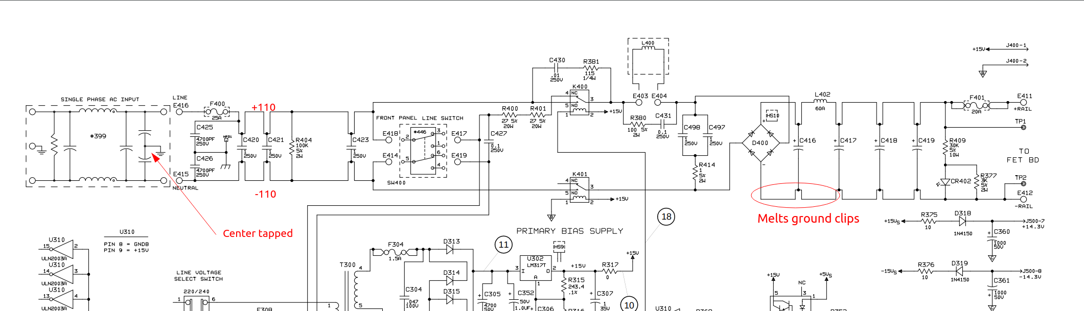
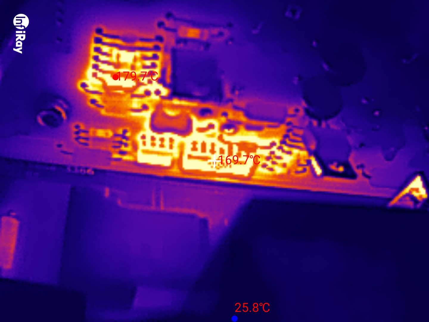
So you can see that the system before the rectifying diode is actually at +/- 110 with respect to the chassis. There is a 10k resistor to the chassis on the FET board:
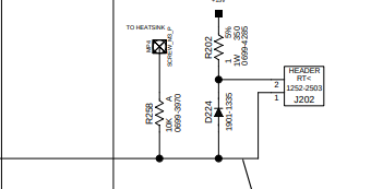
That is sits at 170C according to the thermal camera. . That seems about right for the temperature, but surely the designers of the supply did not intend for -RAIL to be floating so high, given how they tied it to ground.
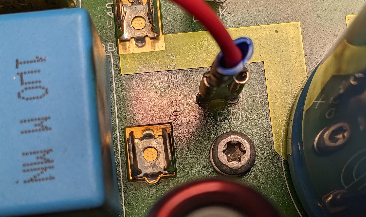
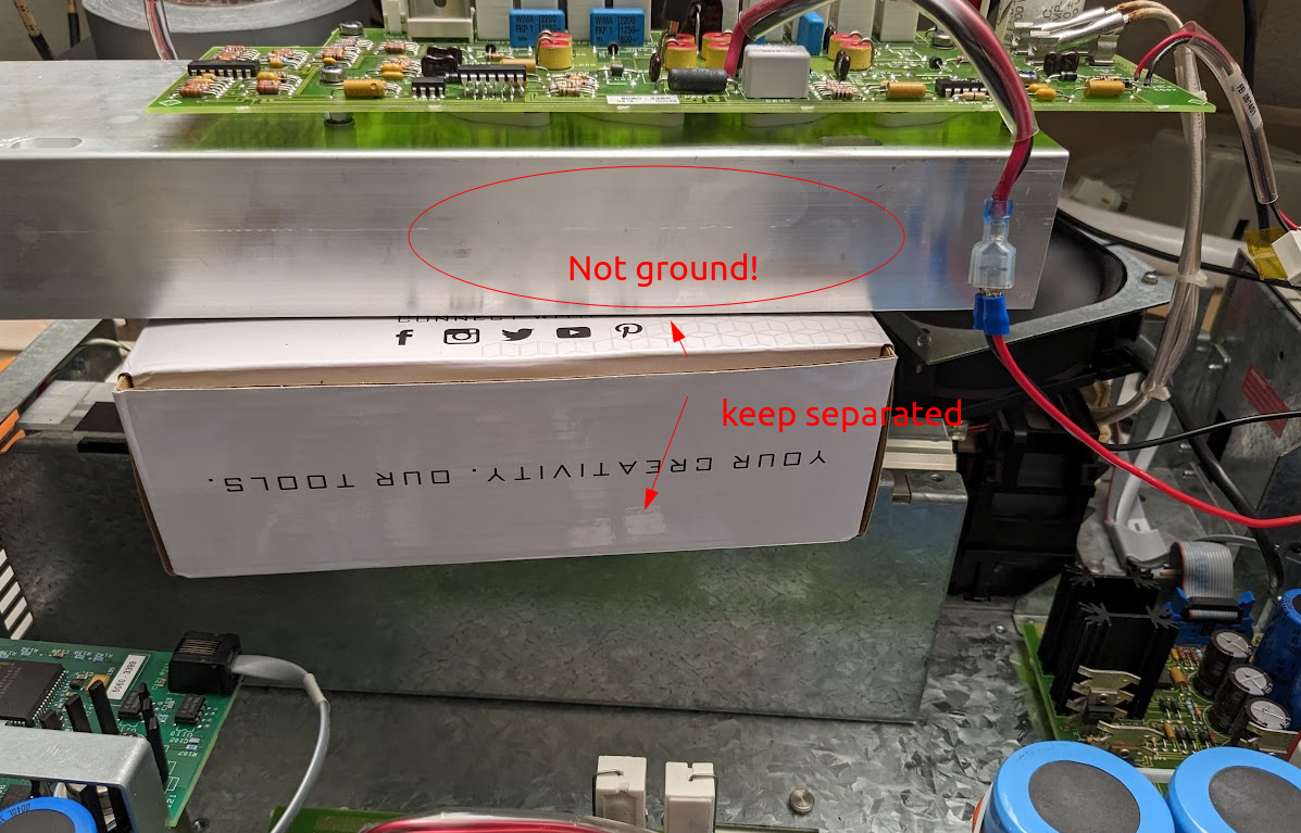
…It turns out that the heatsink is not supposed to sit at ground at all, and that the big plasic clips that hold it in aren’t just there to annoy me but in fact serve to float the whole board. The addition of a printer filament box between the heatsink and chassis drops R258’s temperature admirably:
In order to be able to probe things whilst not being electrocuted I also swapped out the recified mains DC output for a bench supply output of 20V.
Road to success
Bad fmax
The TIP42C transistors that I purchased have a gain bandwidth product of 3MHz:
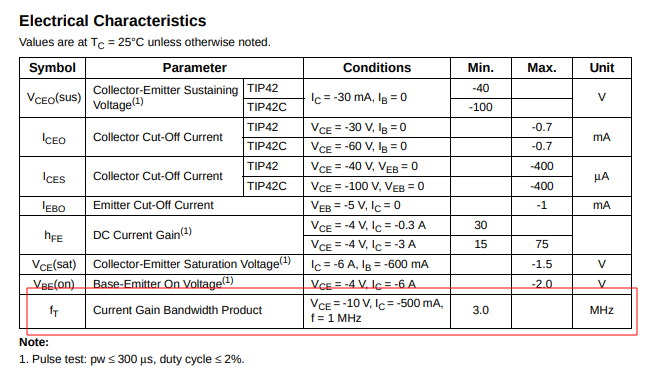
but the original MJD45H11 transistors have a transition frequency of 80MHz:
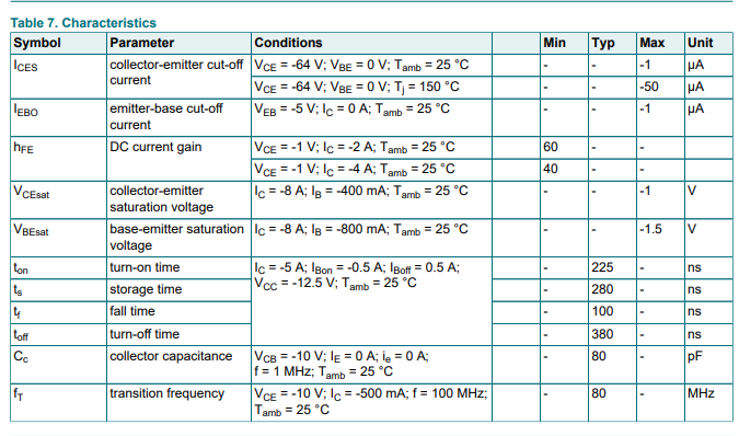
…This would seem to be an issue. So I bought some 2SA1186 ones instead which have a transition frequency of 60MHz, which is hopefully good enough.
More comparisons
In preparation for the above transistors arriving I took all the existing ones off the board, and then started probing about to find further differences between the two sides of the circuit. I discovered that the side with the blown PNP transistor also had some bad power transistors:
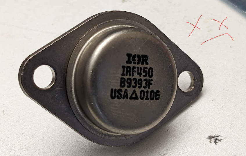
And in addition to that the FET driver that originally died and that I replaced had died again, so I replaced that for a second time also.
All of this was made possible by comparing the two symmetrical sides of the circuit and comparing waveforms to help reason it out. Without that reference to look at I think this would have taken far too long to figure out and wouldn’t have been worth doing.
Unlike what you might expect from looking in the schematic of the manual, the supply actually has two sets of FET’s in parallel:
So I took some working FET’s from side B and put them on side A. In total two of the FET’s of side A were completely kaput and one of them was functioning merely poorly (the waveform didn’t look idential with the other side). After replacing all 3, I got a regulated output voltage! The power board was being supplied with 20V and doesn’t seem to want to go above 5.5V or so but I think that’s OK and should be fixed when I switch back to mains. This regulated voltage was actually achieved without the pnp transistors at all:
So I guess they are just there to speed up the edges. I also think that it would be best to add them before actually drawing any load from the supply.
And now, for a very confusing graph:
OK so it turns out what looks too good to be true is. Even though the output is being correctly regulated, there is still something clearly wrong with the FET driving still:
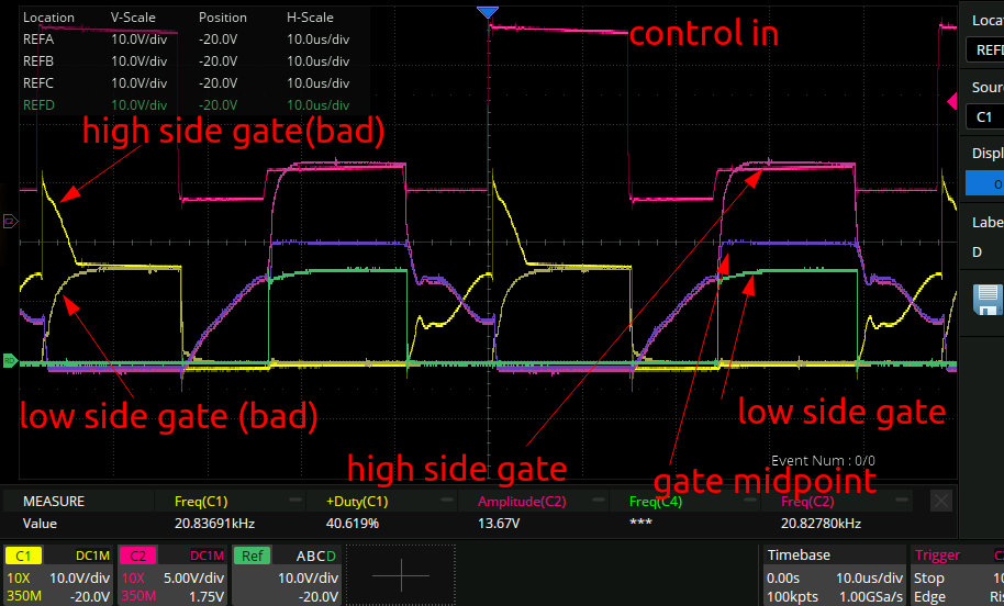
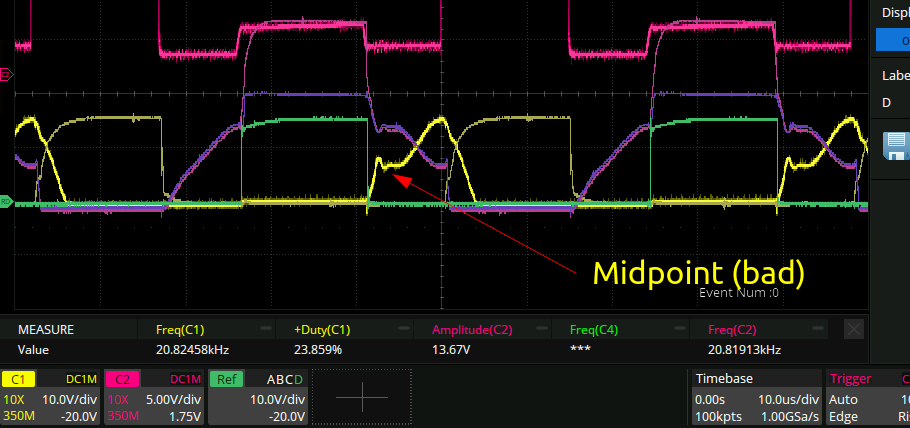
The high side gate of the side of the schematic that has components blowing up is still clearly not being driven correctly for some reason. The “high side gate(bad)” clearly shows this, it is not capable of drivin up to the same as the high side gate on the other side. Here is what the half bridge midpoint looks like:
So if you take the yellow trace in the top plot - the yellow trace in the bottom plot you get the Vgs of the top FET. and clearly the source of the FET is not floating up to any rail at the time that the high side gate goes high. So perhaps this FET is also dead and not conducting? I do have one more spare power FET, so let’s try that.
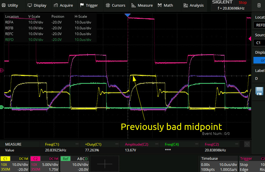
… There we go. I suppose in retrospect it should have been surprising that 3 out of 4 FET’s on a half bridge would fail. But I was fooled because some of them failed short circuit and some failed open circuit. After replacing that last FET everything seemed fine so I put the FET board back on the mains power and nothing blew up. As far as I can tell that means that the unit is working!
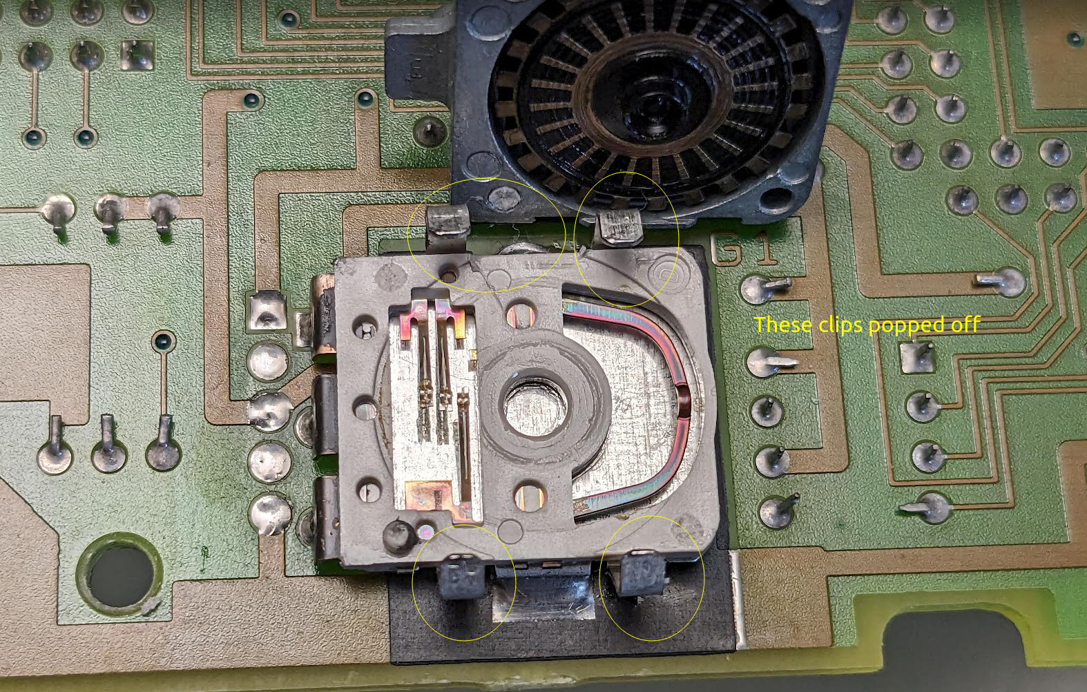
Cleanup: encoder
The two encoder wheels on the front had gotten banged and the knobs popped off:
Inside the encoders look like this:
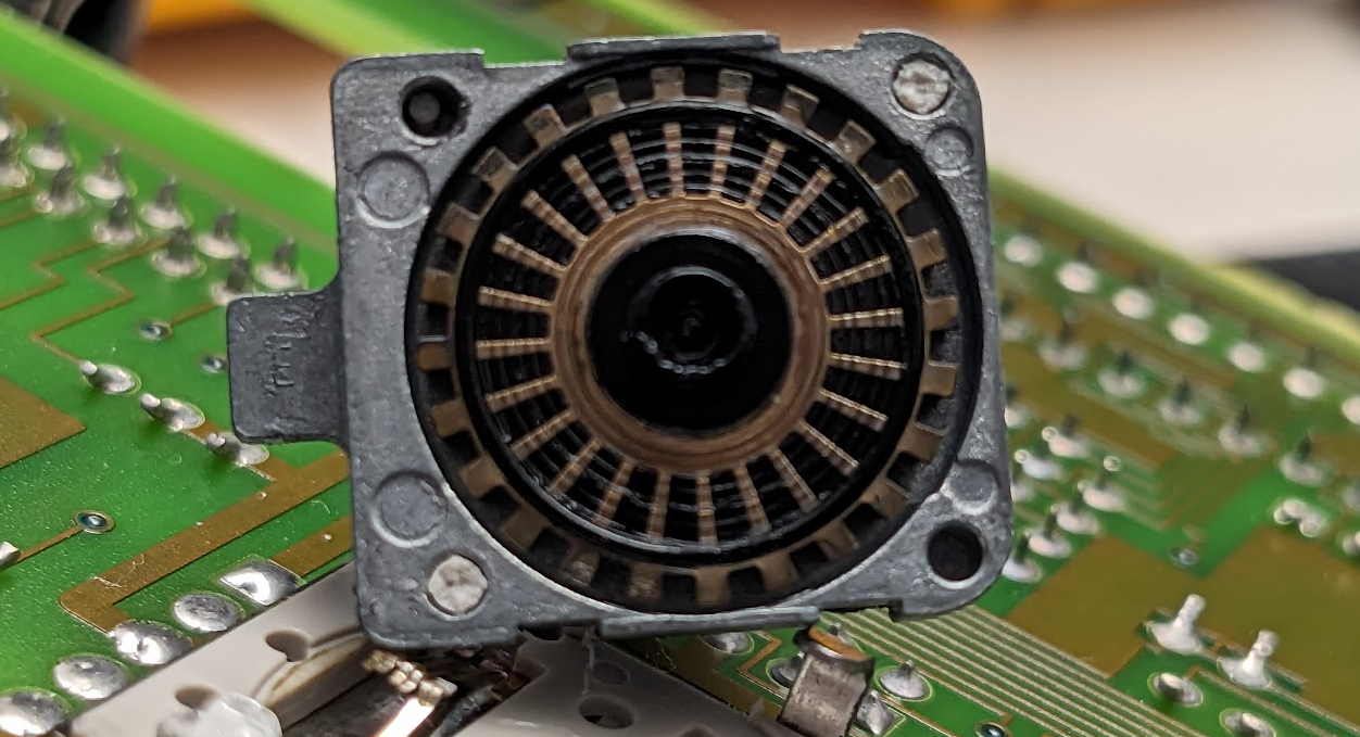
The actual wheel is a very solid piece of metal, basically looks like a motor stator. Seems kind of gratuitous to be honest, but then again the encoders survived the 7mm ABS shaft being snapped off, so what do I know?
The saga continues
I just blew up the supply again. How annoying. This time it seems that both the regulator and the half bridge are dead:
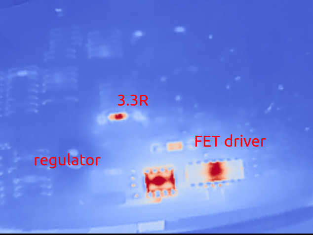
I think that this is the reason the 3.3R resistor was so hot. There was a short through the failed FET driver.
I have ordered some replacement