New PCB looks like this and is made of Aluminium:
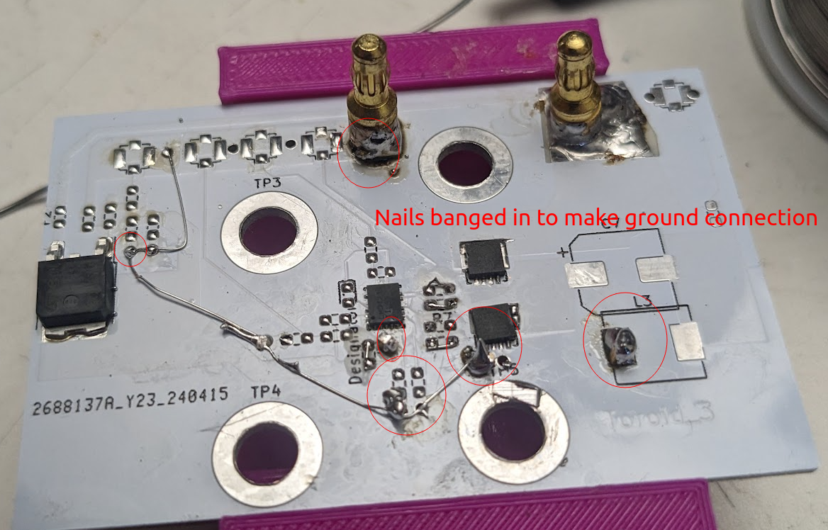
It turns out that when you buy an Aluminium PCB and put vias in it, the vias don’t actually connect the top layer to the ground plane. I discovered however that the legs of a PCB mount SMA connector can be snapped off and hammered into the 1mm holes, and then soldered to. This makes a fine connection.
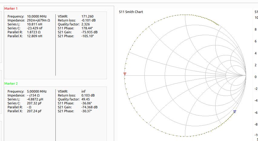
Retuned circuit:
I use my brand spanking “new” power supply to power the half bridges. This worked fine but I never seemed to hit resonance for some reason. So I popped the LC off and put it on the VNA, then dialed the variable capacitor in so the resonance was exactly 10MHz:
After that I tried to solder to the half bridge with the power supply on, and the half bridge blew up. So did the power supply. What a tragedy.
Fixed power supply, analyse usage
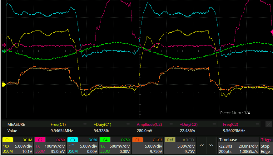
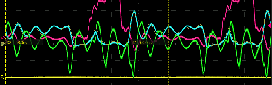
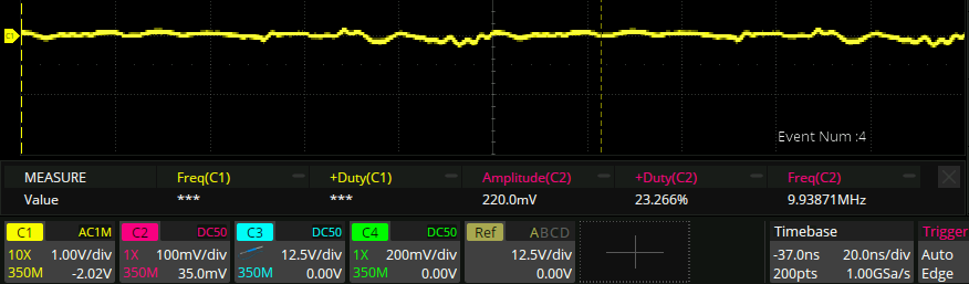
Now I have things back up and running. I noticed that there was a large change (>10deg) in the temp of the MOSFET with a small change in the input frequency from the signal generator. I had initially attributed this to the resonant frequency of the LC, but the fact that only the low side mosfet changed temperature made me suspicious. Here is a screenshot of the half bridge operating at ‘low power’:
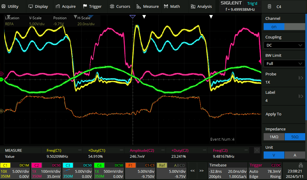
- Yellow: High side gate
- Blue: Half bridge midpoint
- Purple: low side gate
- Green: EM field from a loop nearby
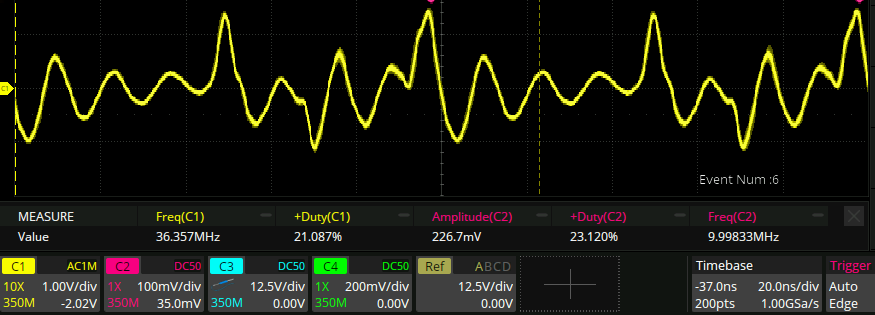
- Maths: High side gate - Half bridge output (Low side gate voltage) And at ‘High power’:
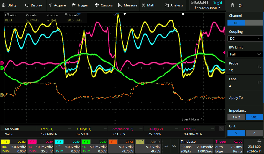
So it seems there is some kind of shoot through happening. Some more observations:
- The magnitude of the EM field did actually increase, but not nearly commensurate with the rise in power dissipation (The current from the supply like doubled here)
- I checked, and there is little time delay between CH1 and CH2 here
- The higher frequency wibbles most obvious on CH1 are highly dependent on local meat placement.I can almost make the “shoot through” disappear from moving my hand around.
- The voltage on the gates would suggest that there should be no shoot through at all.
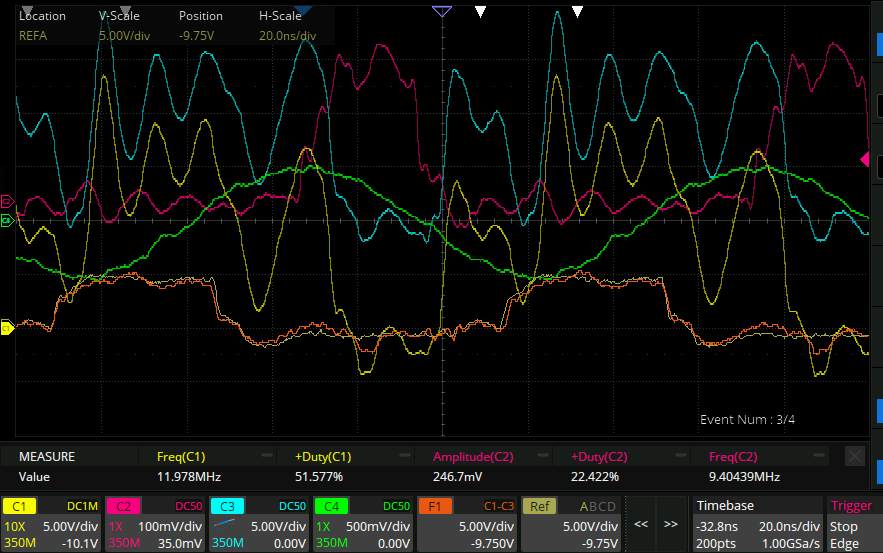
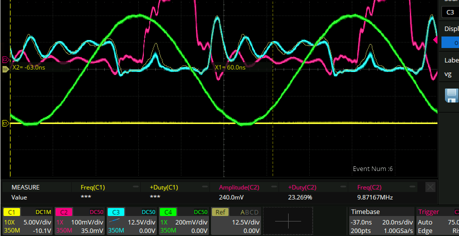
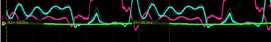
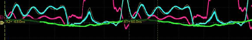
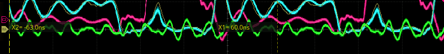
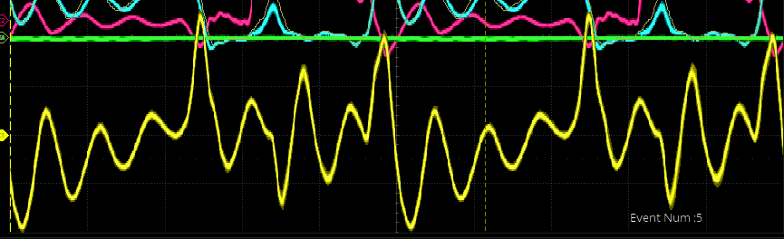
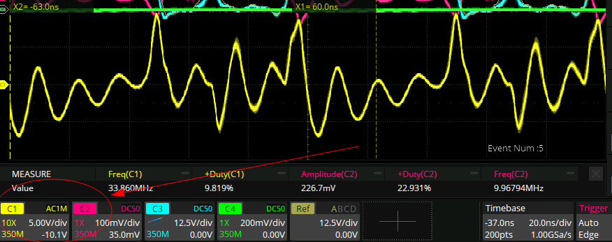
Some more experiments. Here is 9.54MHz, where things look completely sane:
And 9.44MHz, completely wack:
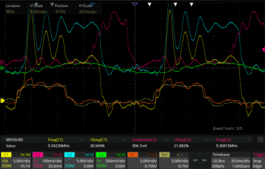
Further down at 9.3MHz, slightly more sane (?):
I wonder where this ringing is coming from. If I can solve that this might solve the issue. In the past power supply decoupling at been a wee bit of an issue so I shall probe the power supply rail. That turns out to have 5vpk-pk ripples in it but I think that’s more or less par for the course at this kind of di/dt, and there doesn’t seem to be an obvious relationship between the ripples and the 80MHz ripples above. Instead I suspect that it is some other LC oscillation in my circuit, though I don’t know where it could be coming from. To test this I detuned things down to where it looks like a nice square wave, then tuned the variable capacitor (with pliers, lest I be burned) and this actually seems to be a good strategy. I get 800mVpk-pk on my field here with the FET’s sitting at a cruisy 45C. Time to switch over to the big boi power supply and crank the voltage!
Magnetic field measurement adventures
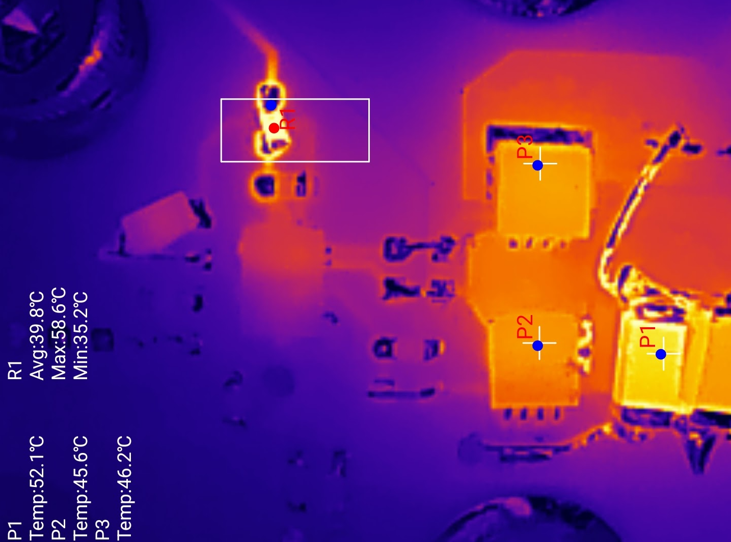
One of the things that I noticed correlated well with the increased power consumption was harmonics/ringing happening on the output waveform:
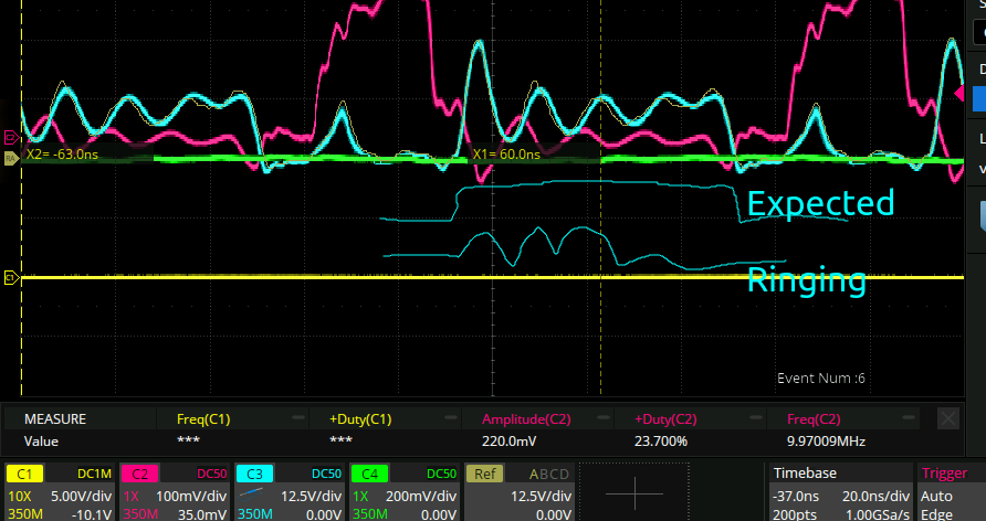
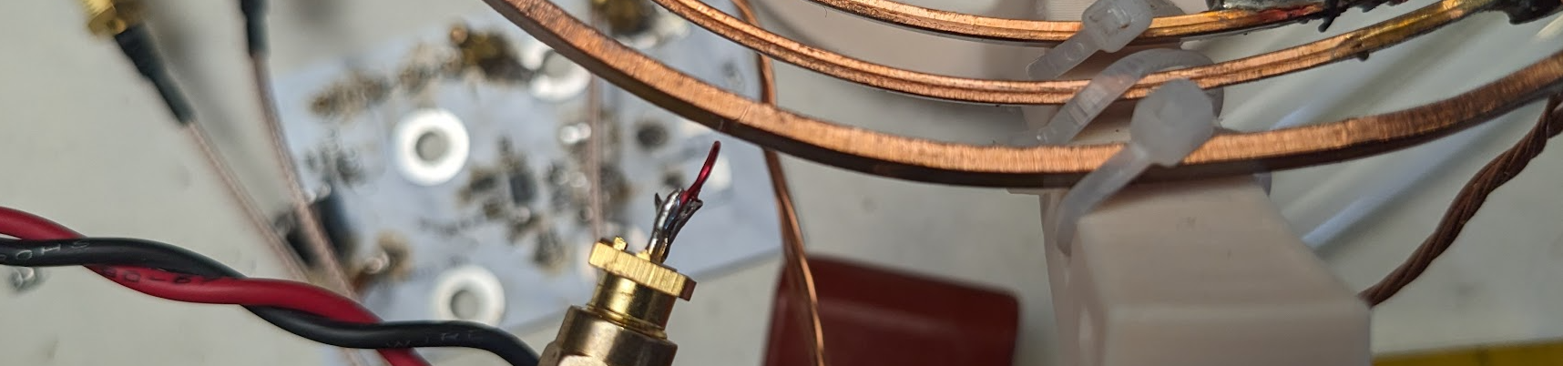
I it was hard to tell where this was coming from. Moving my hand around over the coil influences the amplitude quite a lot. So I made a magnetic probe thingo (loop of wire) to try and find out where things were coming from. Here are 4 measurements:
Main coil field
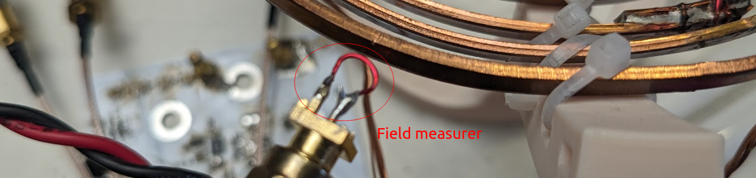
Perpendicular to main coil field
Decoupling cap:
Perpendicular to decoupling cap:
Power supply current:
The vscale on the field measurement is the same in all the pics here obviously. So it seems like a bit clue here that the decoupling is somehow the issue. Obviously the current that created the voltage on the output of the half bridge had to come from somewhere and that somewhere was the decoupling cap. So it could technically be caused by something else,and I am just measuring the supply current to it. But I shall investigate in this direction anyway for lack of anything else to do.
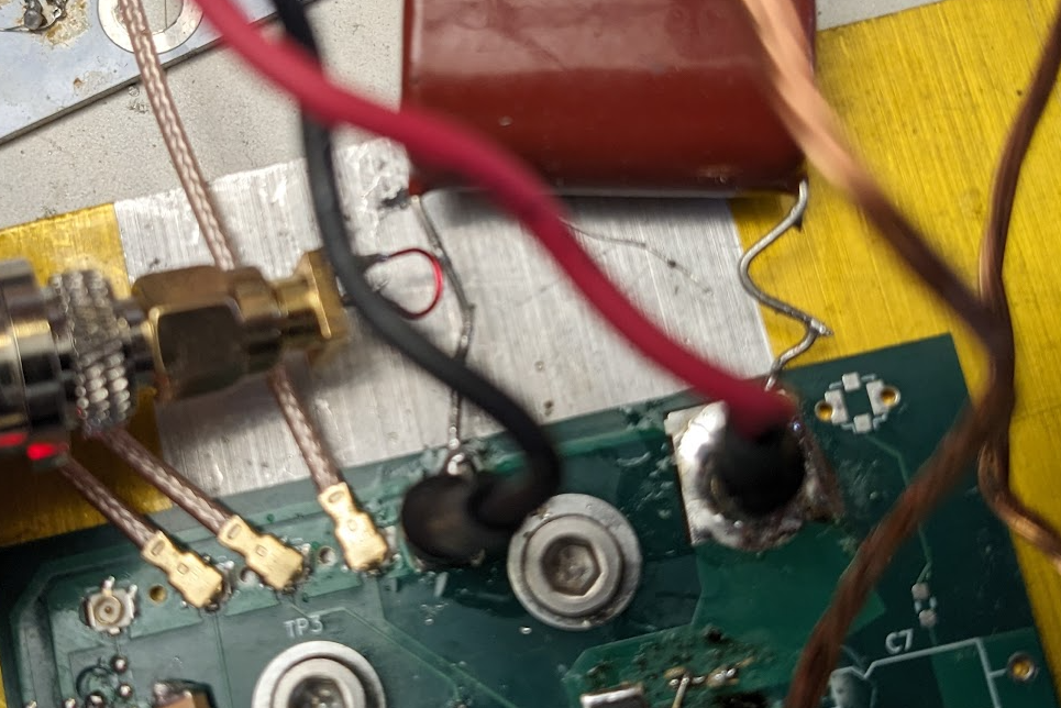
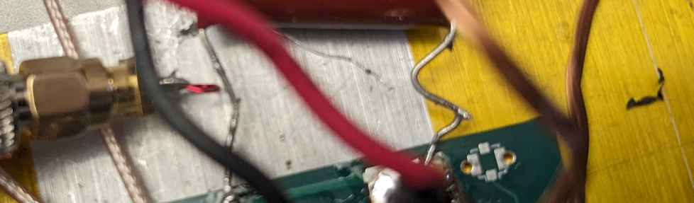
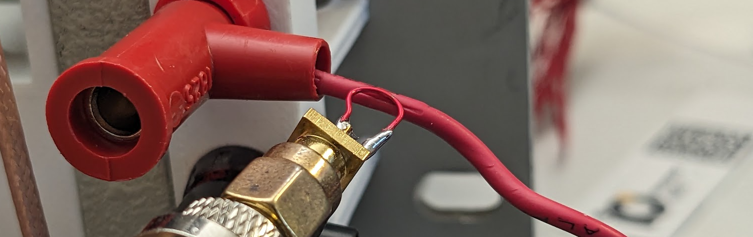
Voltage measurement of decoupling
Because I did not do things properly, the wires for my decoupling caps are attached with wires to ground and to power:
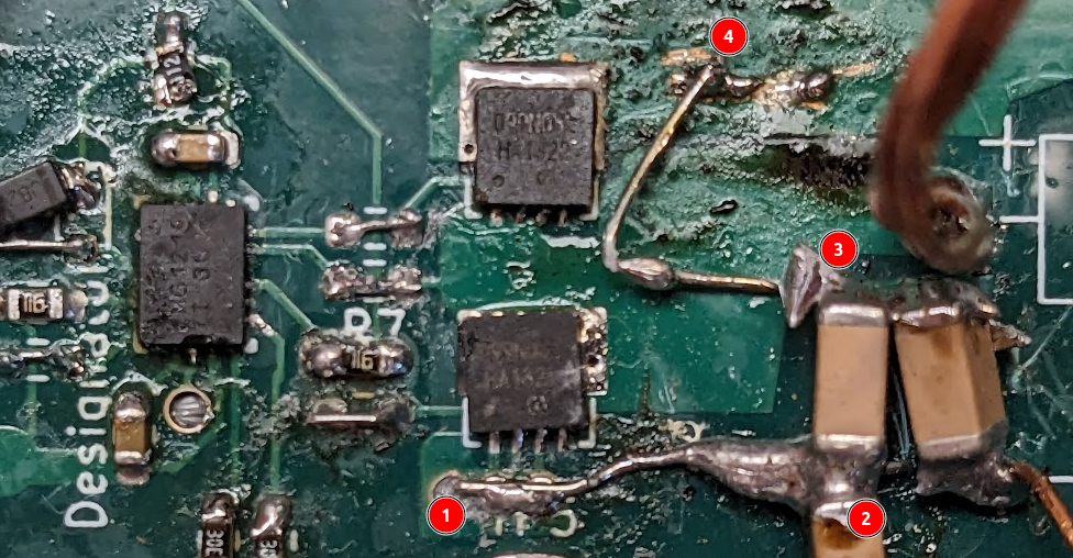
1: ground to ground
2: ground to ground + 10mm of wire
3: Power - 10mm of wire
4: Power
Note that all of these were measured referenced to a bolt ground hole positioned just under the (1) indicator. Obviously on this PCB the ground abstraction is utterly broken. But, measured with respect to a ground hole just to the upper left of (4) VCC looks about the same.