I have spent far too long on the stupid power supply for the awg, time to move on. this power supply I bought is quite neat but woefully underpowered. The one I have on the board is also underpowered. So on the actual AWG board I’ll just leave some 0.1” header pins in the same spacing as the aliexpress board, and will plop down my own power module for now, and can maybe find a better one later.
I would have thought that there would be some super ultra high density modern module thingo I could plop down. Indeed such things do exist, this thing is isolated, can do 30W and is tiny:
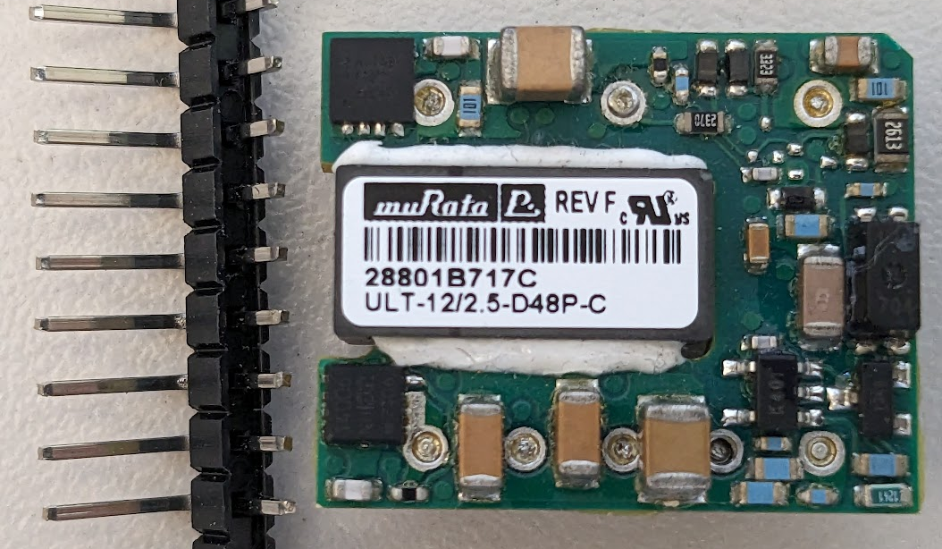
But the modern ones all have a minimum input range of like 36V. When I filter on the same website for stuff that can take 5V as an input the modules are all much worse.
So, I’ll keep the analog supplies as a separate board and can do stuff like supply a barrel jack option and so on for now.
Limits of the analog electronics
This means then that I should set the current limit resistor on the actual amplifier according to the heat dissipation capacity of the amplifer, and not the power supply. Here are some tables of measurements to try and find the highest temperature configuration:
Into 50R:
- Ramp -10V to 10V: 55C, power transistors aren’t even the hottest
- -10V, +10V DC output: fine, around 60C
- max amplitude square wave with period 1 sample: op amp gets to 99C
into 10R: DC -10V gets way to hot. it looks like without a heatsink, the power transistors can do 600mA and only get to 80C or so, but at 700mA they rapidly go over 100C.
Changing the current sense resistors to 1.5R seems to be a good compromise. I’ll leave it at that I think.
One more thing
When adjusting the high side current sense resistor to 1.5R I noticed that the power supply was still doing the current limiting when a high output voltage was commanded. Increasing the current limit on the power supply just made these low side transistors get hotter:
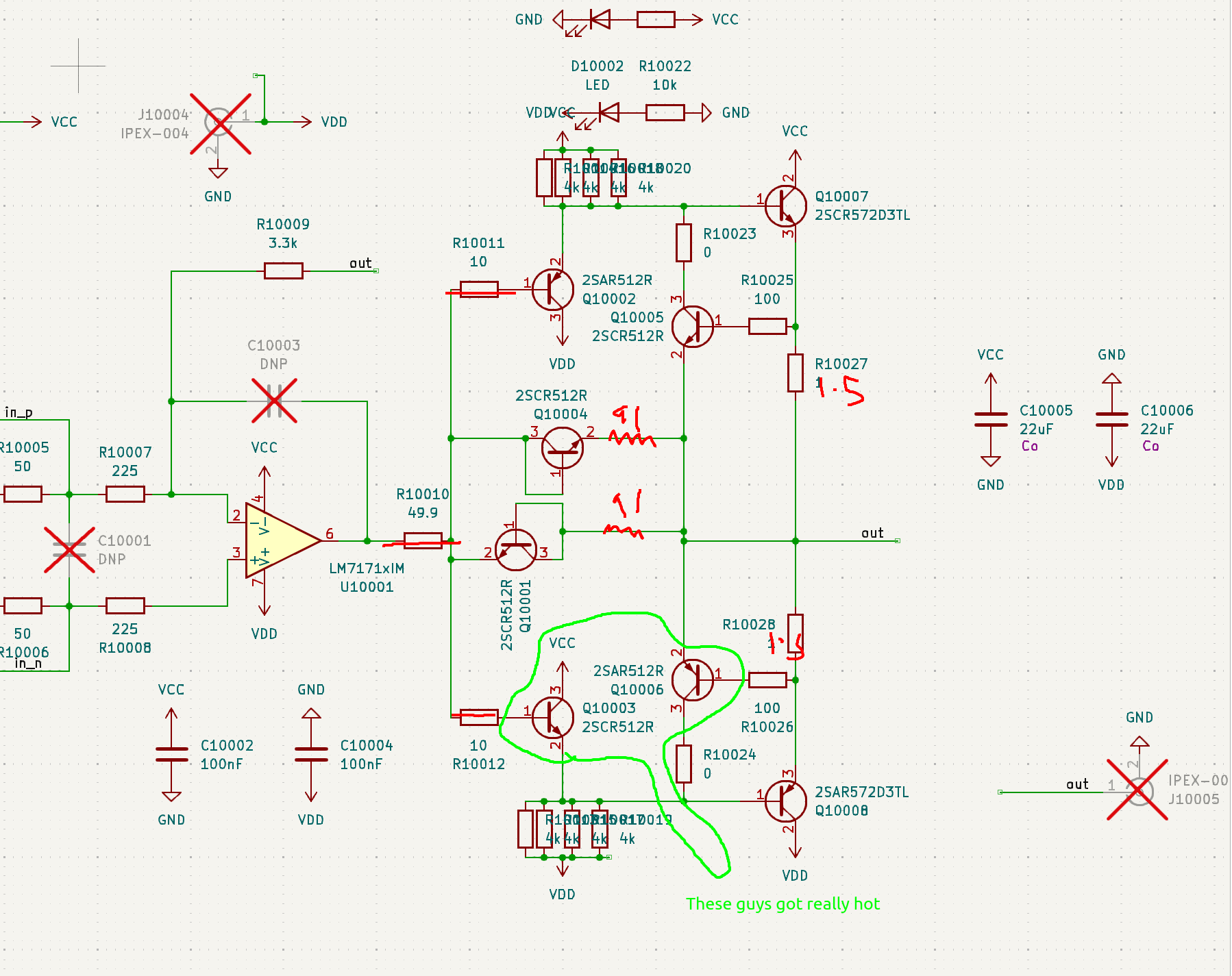
This was rather confusing. I further increased the high side resistor to 3.3 ohms and indeed this made the high side drive FET Q10007 there cool, but the low side transistors were still hot
Reason
This problem occured at DC so I could just probe everything out with the multimeter, which was nice:
It appears that when I installed the 91R resistors earlier to stop the oscillation, I also introduced a problem that required me to understand the actual purpose of the diodes in the first place. Indeed they are required for a short circuit condition. Under that condition the output of the op amp can swing high, so that the voltage at the base of the low side power transistor is higher than at the output. Under these conditions quite a lot of current begins to flow through the low side turnoff transistor, which explains why it was getting to >100C. I don’t 100% understand what’s going on here though since the current shouldn’t be able to flow from the collecter to the emitter, and it is not flowing out of the base as there is only 1V across the 100R base resistor.
So there cannot be a high DC resistance in that loop, the oscillations must be suppressed some other way. Maybe I can stick some ferrite beads there, and then make the resistor on the output of the amp high again, idk.
I can’t see the oscillations right now so I’ll just stick a 0R resistor in the footprint and call it a day until it comes back I think.
Time-averaged current limit.
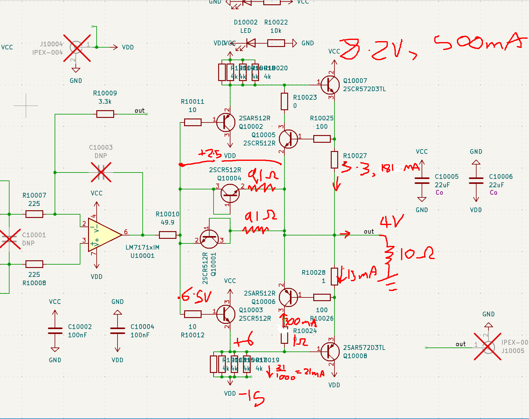
Now that the current limit is working well, I thought it might be improved by being a time-averaged current limit. The current arrangement works extremely quickly, but it actually only has to work on the same time constant as the thermal time constant of the electronics, a second or so. So I thought it should be possible to do this:
By sticking a cap between the base and emitter of the turnoff transistor, you could get an RC time constant set up. Since the voltage across there would only ever be 0.6V you could have a super fat transistor, too.
But when I actually try this by making a waveform with a pulse in it, the magnitude of the pulse doesn’t change at all when I add a 10uF cap and up the resistor to 1k. That should be a 15s time constant! My probing situation isn’t really good enough to get a good measurement between the transistor base and the output so I will again stick a footprint in and leave it at that, gotta get this show on the road.
To LCSC
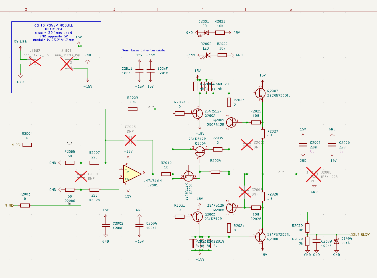
This is the final schematic of the power stage that I ended up sending to LCSC:
I just asked Mr deep research about how one would go about a 100MHz 10A output stage, and got a link to a great TI app note where they just stick 4 amplifiers in parallel. That’s 4 of a $12 part though, so it would be nice to not do that.