The PCB
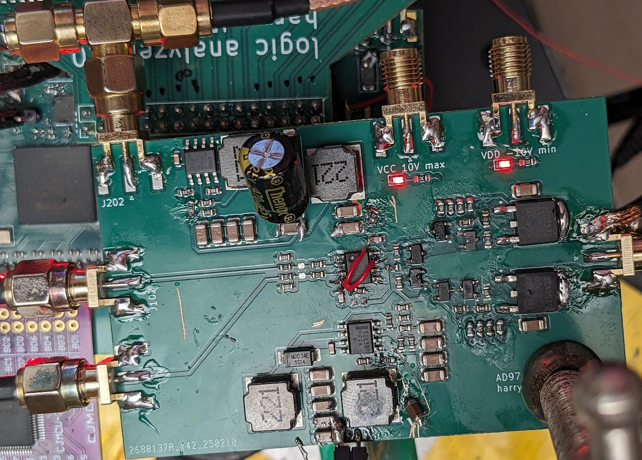
Basically the same as the previous one, but with the changes integrated and the addition of the positive and negative rails for the op amp. The rails look like this:
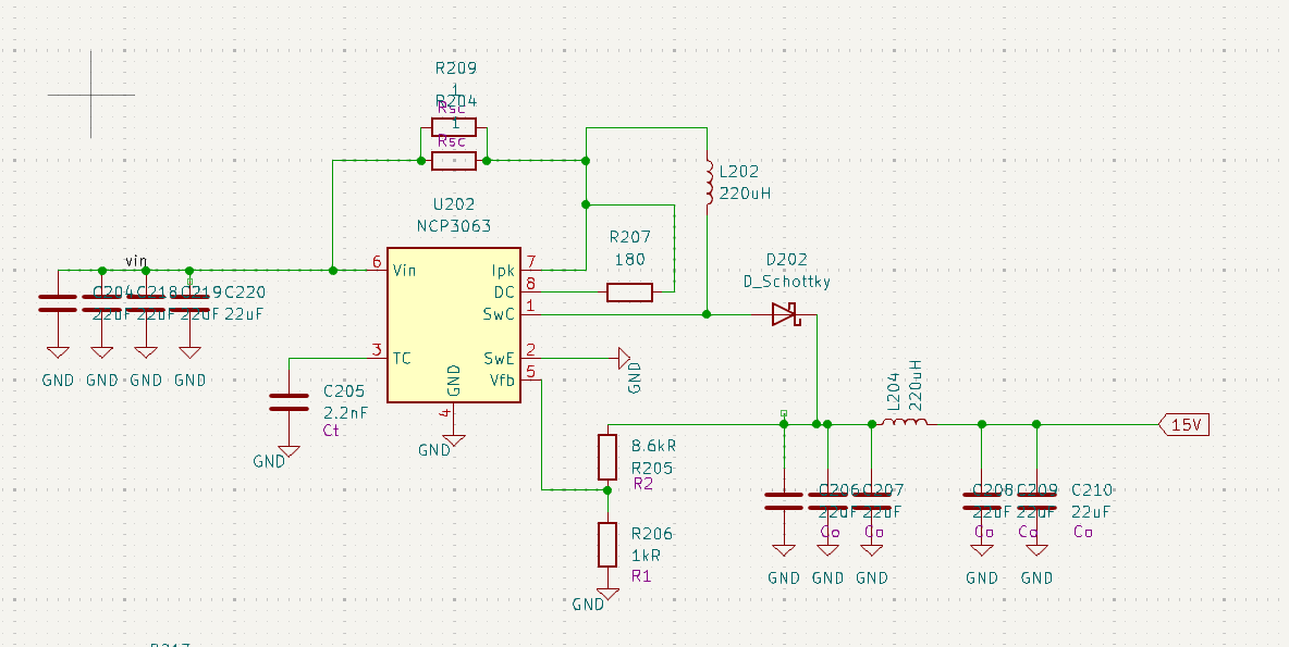
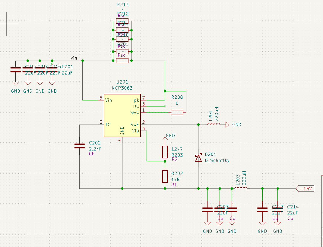
I asked claude to generate all the component values for this based on the datasheet and didn’t bother to check them much. As a result:
Changes required
Voltage level
Need to change “R2” to 11k for both power supplies since the formula for the output voltage is:
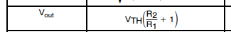
Vth == 1.25V.
Power rail flip
I got the inverting and noninverting inputs wrong for the amp before, so I selected the amp in kicad and pressed ‘y’ to flip it in the y axis:
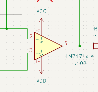
…yeah, that was a mistake.
Bias resistors.
For some reason the bias resistors:
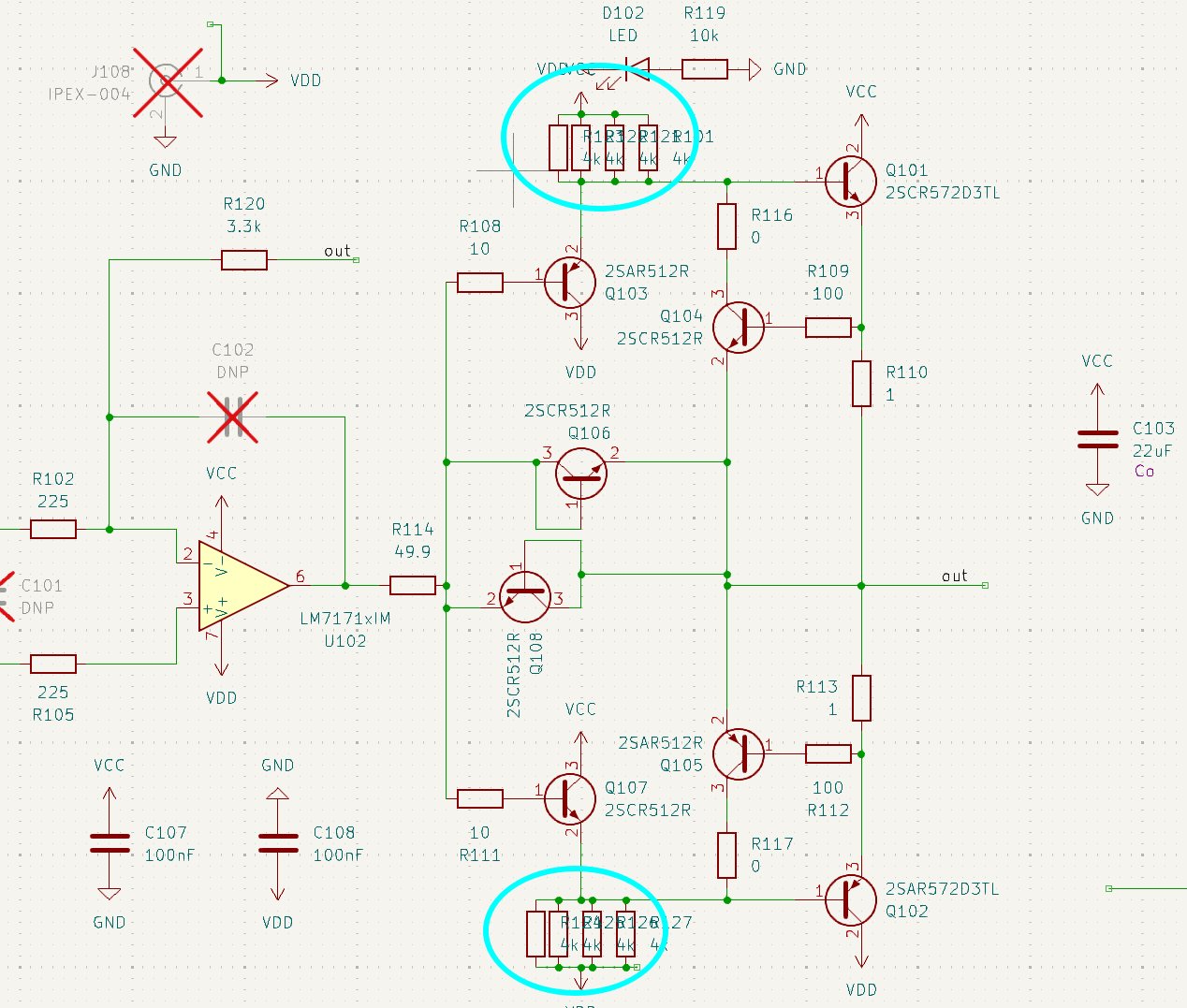
were specified to be 330R each, not 4k. Thermal camera saved me on that one I think.
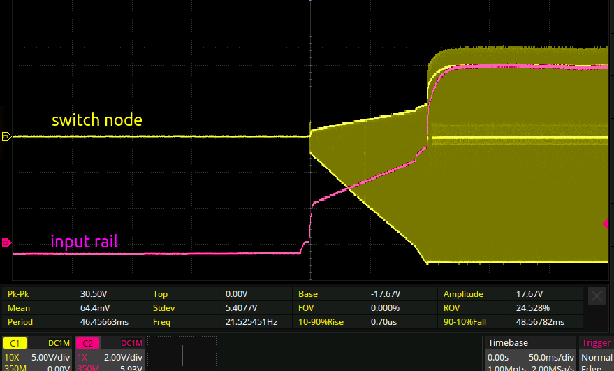
Weird startup behavior
About 80% of the time the negative rail comes up fine. 20% of the time it hits my power supply current limit of ~600mA at a 1.9V input voltage. The switch node looks like this at this time:
Don’t know why this is, but it’s clearly just shorting the inductor to ground permanently. I noticed that the example schematic had 470uF on the output instead of my 60uF so I added a 470uF electrolytic too. That seems to have fixed the problem. I assume that if there isn’t enough capacitance in the system the inductor will discharge itself in less than one switching cycle or something like that and get the chip into a bad state.
…Actually this did not fix the issue. There are some super weird correlations going on. It’s almost as though the temperature is important, it seems more likely to happen right after soldering something on. But it also might just be that it happens more often after waiting a while. There definitely don’t seem to be any caps that take a while to discharge, so it isn’t that.
I thought that perhaps there wasn’t enough input capacitance, and so the voltage on the input was going really low on the first switch of the power supply, and the subsequent switch never turned off and shorted the inductor to ground. It isn’t that either, I can see on occasions where it ‘works’ the power rail goes up to 2V, and on occasions where it doesn’t work it just goes up to 10, monotonically in both cases.
This is what a successful startup looks like:
and an unsuccessful one (had to zoom in a lot):
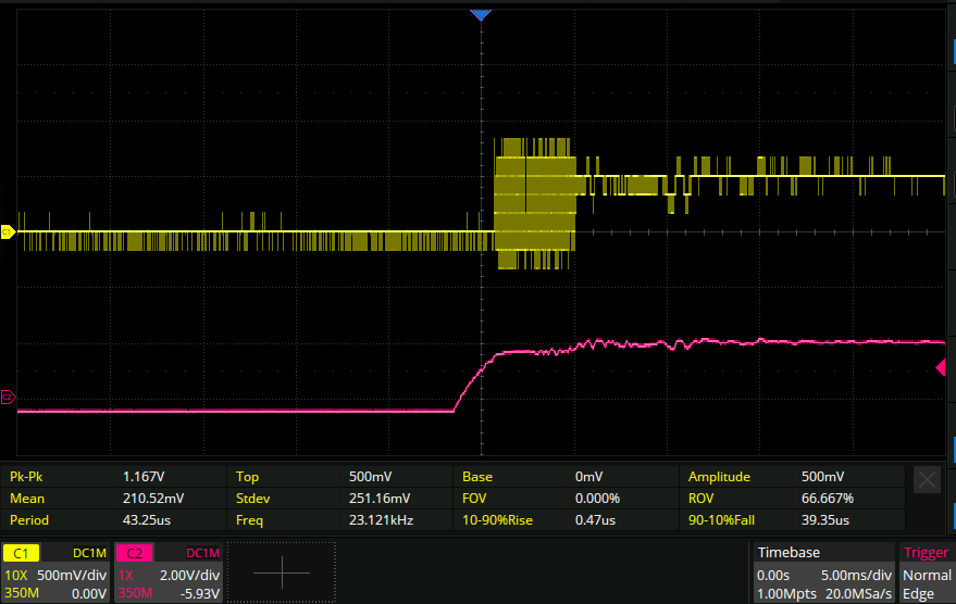
I also tried adding a 10uF cap to ground on the feedback pin for a “soft start” per ChatGPT, but that did not work. What actually is the problem is that this particular power supply turns on too slowly. I’ve been turning my pcb off and on using the main switch on the power supply, and that gives a ramp rate of what you see in the first picture above. If instead I just jam the SMA connector into the power supply after it is turned on then the rise time is much shorter and everything works fine. I guess if the output switch turns on at a voltage lower than what’s required to hit the ‘off’ condition then it really is just a short to ground.
Now after hot gluing on my own switch things are 100% reliable. When it is in actual use powered by a USB or something else, it will have the full rail voltage available straightaway.
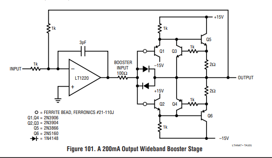
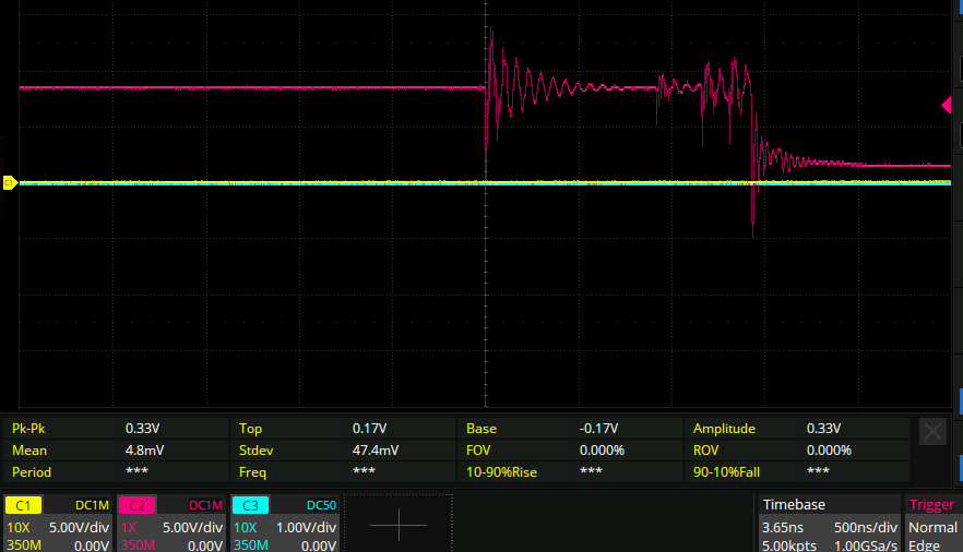
Oscillation
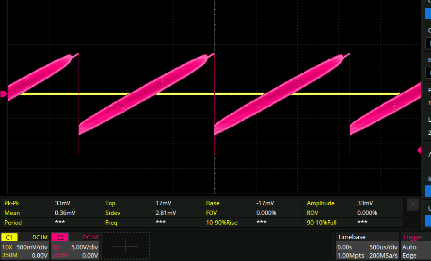
This is what the output looks like with a ramp fed in and the power supplies working:
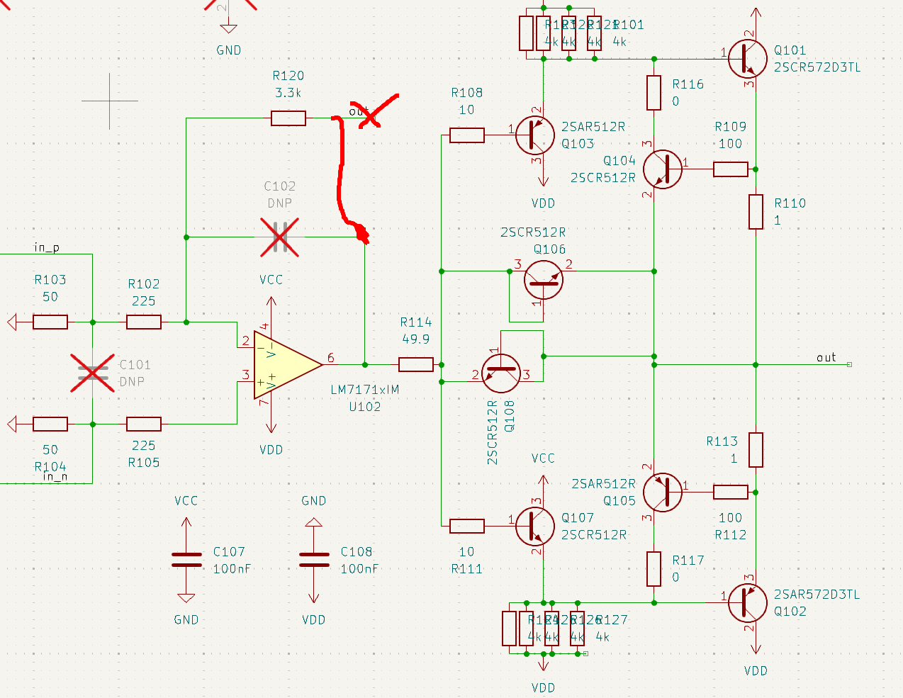
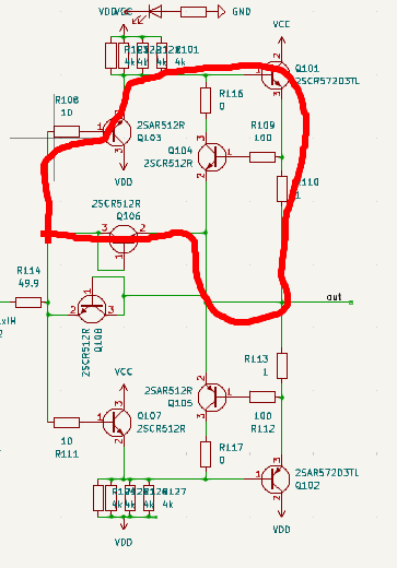
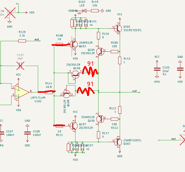
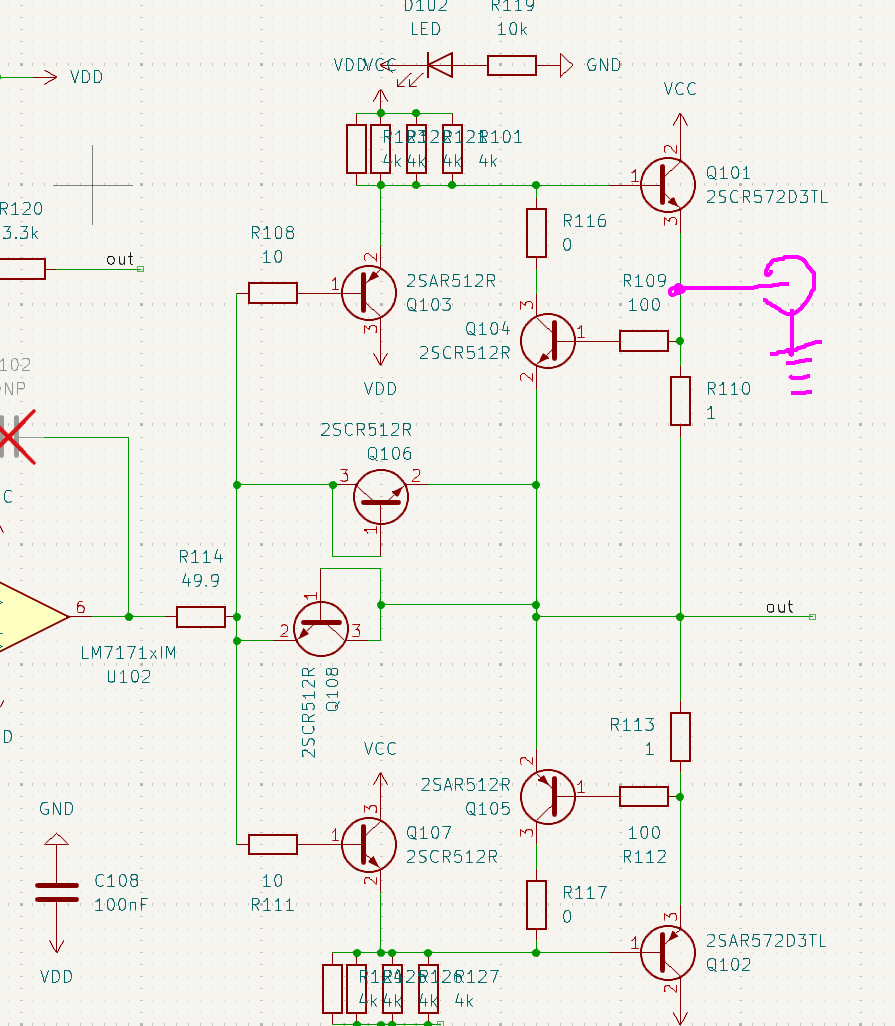
Per Jim Williams AN47 in the previous bringup, this is very likely the larger power transistors being slower somehow, despite the fact that they worked fine when I deadbugged them on the previous rev of the board. There is no oscillation present when the output is 50R terminated though, I wonder why that is. Time to measure the rise time. Here is the change I made, so the op amp excludes the booster circuit from the feedback loop:
(actually just moving R120 into the C102 footprint). Interestingly the oscillation is still present! It goes away if R114 is removed. It also takes a second or so to come back after power on, which is interesting. The frequency is around 50MHz.
Ferrite beads
Let’s see if replacing R111 and R108 with ferrite beads per the app note:
works.
using a 600R@100MHz ferrite in an 0603 package I get this:
…Rather the wrong direction, that. Shorting out the ferrite entirely actually makes it a fair bit better. I also noticed that the oscillation is extremely temperature dependent. A whiff of condensed air spray makes it huge, and a whiff from the hot air gun makes it go away. ChatGPT informs me that the gain of a bipolar transistor goes up as a function of temperature, so that might be it.
From poking with the soldering iron and the condensed air can, it is clear that Q103 and Q107 are indeed responsible for the temperature dependence of the oscillation.
Since the DC resistance of the ferrite bead is ~0, and I replaced a 10R resistor with it, I thought maybe the worsening of the oscillation came from the drop in DC resistance and not from the ferrite beads ferritey properties. So I put a 10R resistor back in, this time in series with a 60R@100Mhz ferrite (instead of 600R@100MHz) so as to have a lower Q. This makes the oscillations quite a lot worse than with the 10R resistor, which doesn’t make much sense to me.
No input required.
Now, the booster stage seems to be quite happy to oscillate (with a many volt amplitude) when it’s all by itself. The only requirement is that a 1m coax cable is attached to the input (so 100pF ish), and the cable on the input is not terminated. When that is the case, it will oscillate even if the output is loaded with 50R.
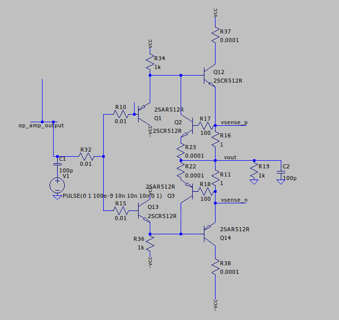
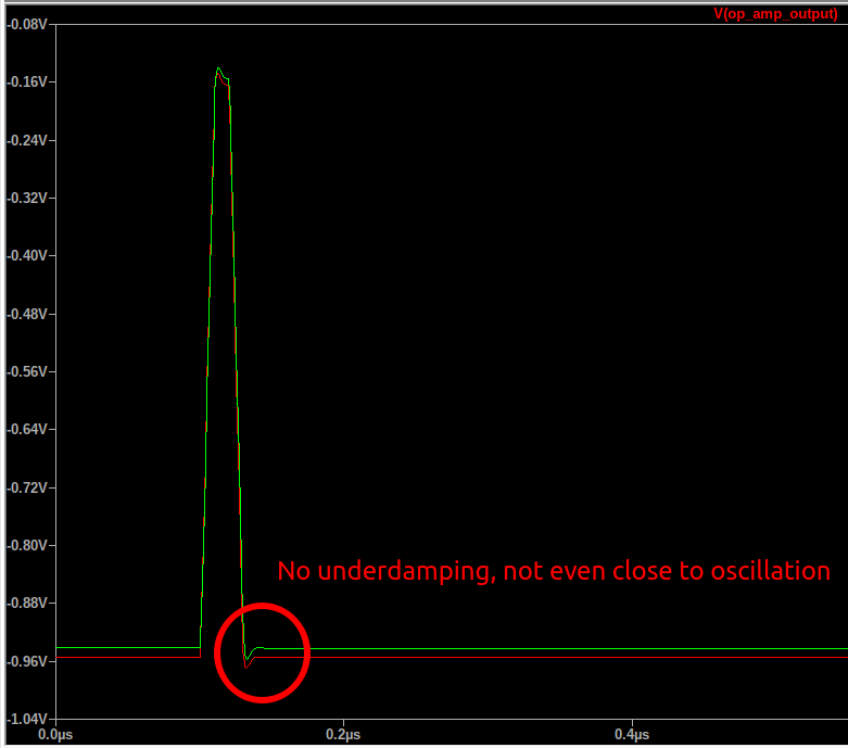
I decided at this point to simulate things. Since my windows VM has also kicked the bucket I went and installed wine to run LT spice. I am not able to get the simulation to oscillate, surprise surprise. Tried adding various capacitances to the input and output, to no avail:
Power supply aside
I disconnected the base resistors R108 and R111. when either of them is disconnected, the power supply reliably exhibits the “shorted powerup” issue of before, even when the rise time of the input is as fast as my mechanical switch can go:
Most things are obvious, once explained
The circuit oscillates. So, it must have a feedback loop some where. Where is there a loop on the schematic?
Duh. Removing Q106 and Q108 stop the oscillation in its tracks. And I just realised above that I didn’t even put those diodes in the simulation (because it was a sim of rev1 of the board). Unfortunately, adding them in properly does not reproduce the oscillation either, so I will have to debug in the real world as per usual. First step is adding a hefty resistor from the output side of the diodes to the actual output. That way I can keep R114, R108, R111 a ~0R, whilst still adding a lot of damping in the feedback loop. I wonder if my choice of a diode-connected-transistor here rather than an actual diode is what is enabling the oscillation somehow, but don’t see why.
Anyhow, this change fixes the oscillations completely:
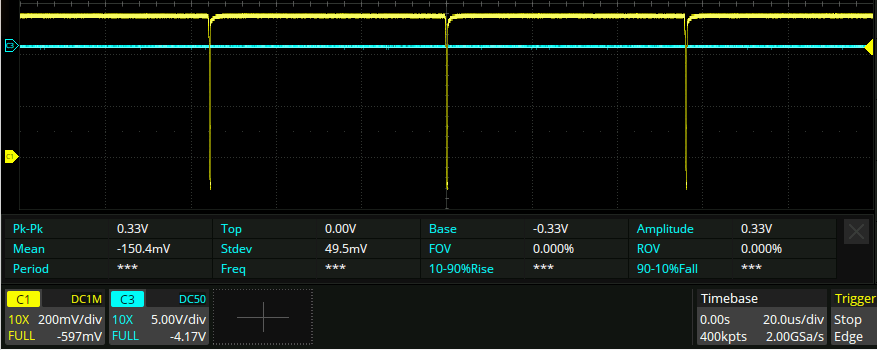
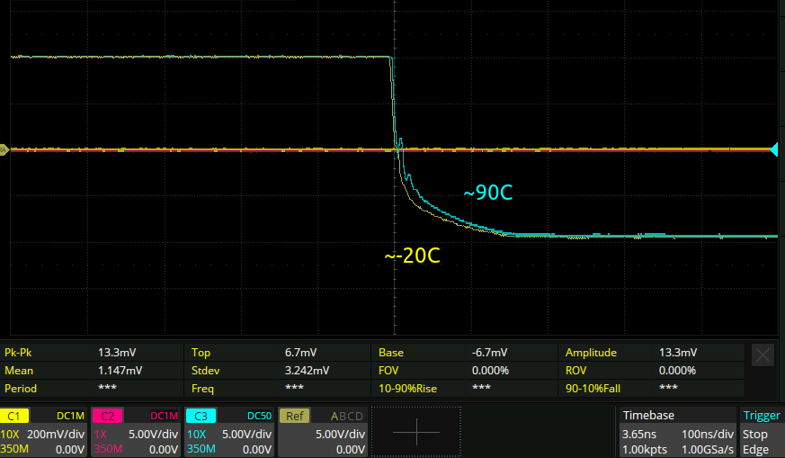
The difference in performance of the fall time over temperature:
10R loading fail to start supplies
Since the amplifier works properly now apparently, time to test it under load. Adding a 10R power resistor to ground makes the amplifier fail to start up though. However, starting the system and then attaching the load yields this result, alongside a 130 degree negative rail chip:
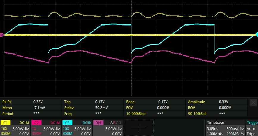
Where the top and bottom trace are the positive and negative rails, which should of course be at 15V. At this time the current sense resistors on the booster stage look like they have around 300mV across them, but not enough to turn on the current limiting funcitonality.
Here is the AC coupled voltage on the low side of the negative voltage rail:
So it looks like the current limit is kicking in here on the negative rail. Probably the positive one too.
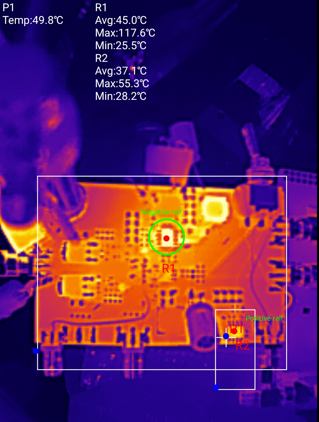
However, the negative rail IC is currently sitting at 117deg. The perfect temperature, I wouldn’t dare put it any hotter. The inductor is also cooking at a decent temperature too!
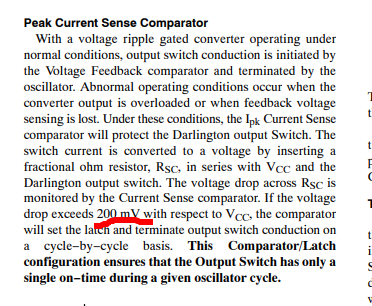
The power output of the IC is defined by the “switch current”. I take this to be the definition of the switch current:
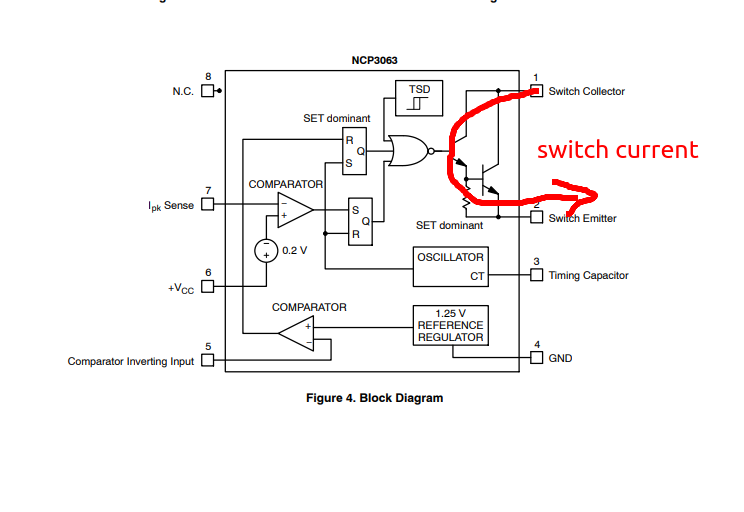
because it makes sense, and because the datasheet says the switch current is measured by the current sense resistors. However the total switch current for both amplifiers combined is 1A as measured by my bench supply. So I don’t see how I can be exceeding that here. Here is the table of the efficiency for the inverting configuration in the datasheet:
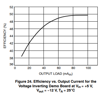
???? It’s only 50%??? What? All the other configurations are like 85%, so I just assumed that the inverting would be the same!
External MOSFET
Perhaps I can increase the efficiency, or at least move the heat out of this poorly heatsunk SOIC-8 package by adding an external transistor. The datasheet does not have information on how to do this for the inverting converter, so I did this:
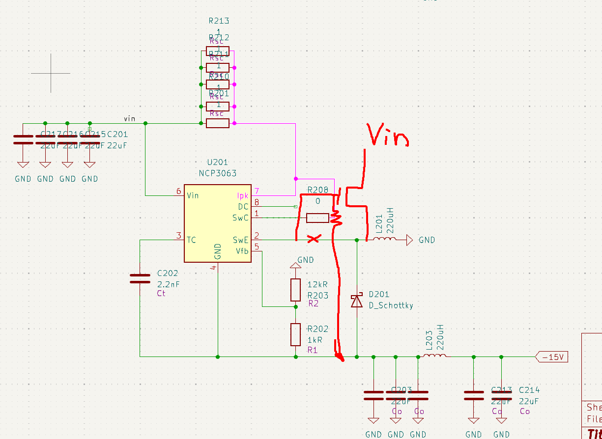
This does not work and had me puzzled for quite some time. With no load connected the output only gets to -8V. However it transpires that this is for headroom reasons. The input is only 5V. The top of the inductor can only be driven to (5V - switch voltage drop - MOSFET threshold voltage) which is like 2.5V. And the MOSFET isn’t even hard on, because the source of the MOSFET wants to float up to the supply.
Increasing the supply voltage to 10V means that the regular can achieve its desired output voltage of -15V. But attaching a load brings that downs to -10V and also puts the MOSFET at around 140C, most likely because the source will always float up to where the gate is. I wonder if I powered the NCP3063 off the 15V rail, and put the MOSFET drain at 5V. Then, the source would float all the way up to the 5V supply rail since the gate would be at 15V. That’s worth an experiment.
I performed this experiment by changing the input voltage to 10V, and then powering the drain of the external FET from a 5V supply. This succeeded in regulating to 15V fine, since when the supply switch is conducting, the gate is driven to +10V, with the source sitting at the input voltage of +5V. When the switch is no longer conducting, a 100R resistor pulls it down to the negative rail of -15V, so the gate is turned off properly.
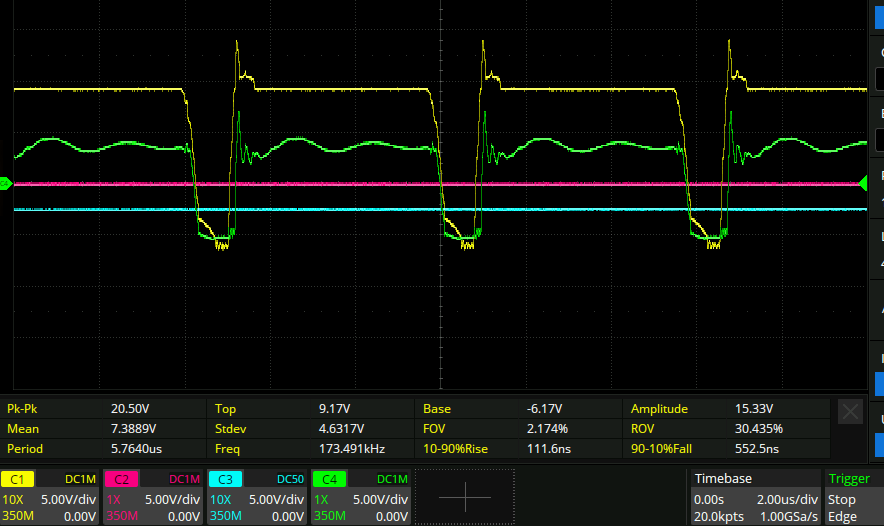
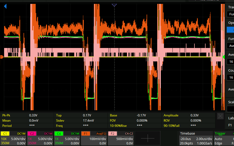
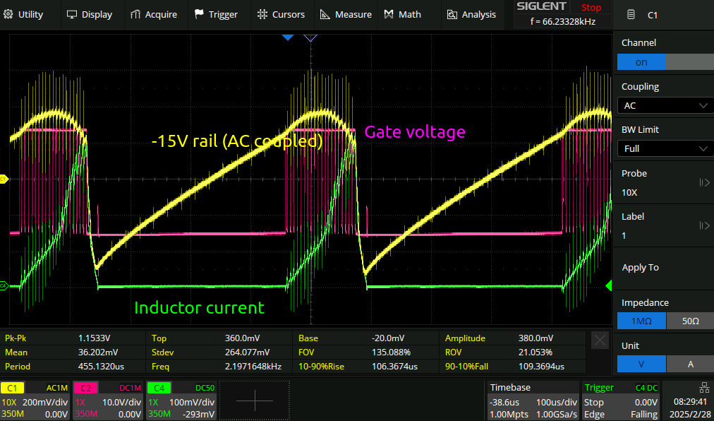
With no load, the max temperature of any component is 47 degrees. With a 10R load on the output, the op amp can’t swing past about +/-5V or so, and the inductor gets up to 160 degrees. Toasty! The waveforms on the gate (yellow) and the source of the FET (green) look like this:
This isn’t exactly textbook, but also I don’t see what could be done to improve things here. The inductor I am using is this one:
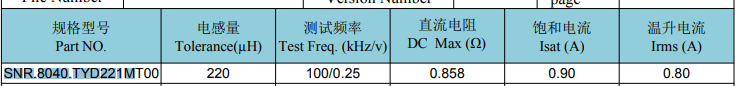
I’m drawing an average of like 1.5A here, so that isn’t great. I need to figure out if the inductor is doing the right thing here.
Art of electronics
The art of electronics (still better than an LLM!) has this to say on the topic:
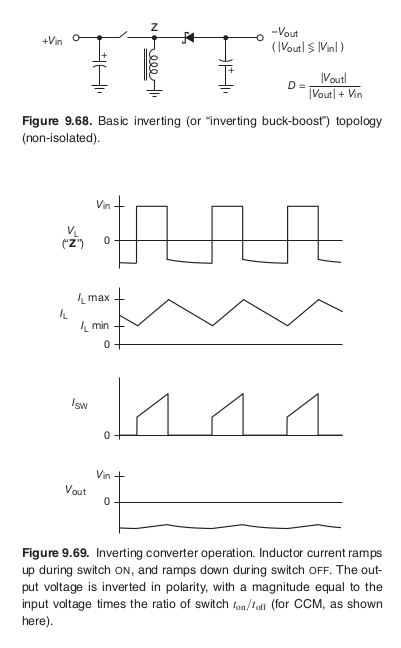
So it looks like I want to measure the current going through the inductor somehow, and see if it has a sawtooth. Deviations from that presumably mean something bad.
The art of electronics says that the minimum inductance is:
Where T = switching period.
Which in my case given a 60us switching period is (60e-6/2)*(15/0.5)* (5/(5+15))**2 = 56uH. My inductor is 226uH which might be a bit high I suppose, but not unreasonable.
I connected a stainless steel strip between the source of the FET and the switch node. It’s around 0.1R I think but I’ll measure it later if it’s important. Channel 2 and 4 measured either and, and math was used to subtract.
Here is the current going through with the supply powering the circuitry, but only a 50R load on the output:

And with the supplies disconnected from the booster circuit, so the load is 0:
Well then. It looks like what I’m measuring is the difference in gain between the two channels. This is what the current looks like when I measure using a sense resistor attached to the bottom of the inductor:
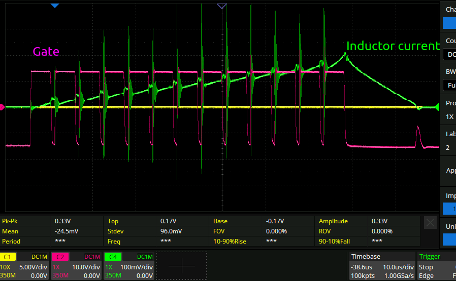
Looks like the supply is only switching once in a while. This is what it looks like with the booster circuit hooked up with a 50R load:
Actually all of the above was done without the waveform generator putting in its customary ramp wave. When that’d done things looks different:
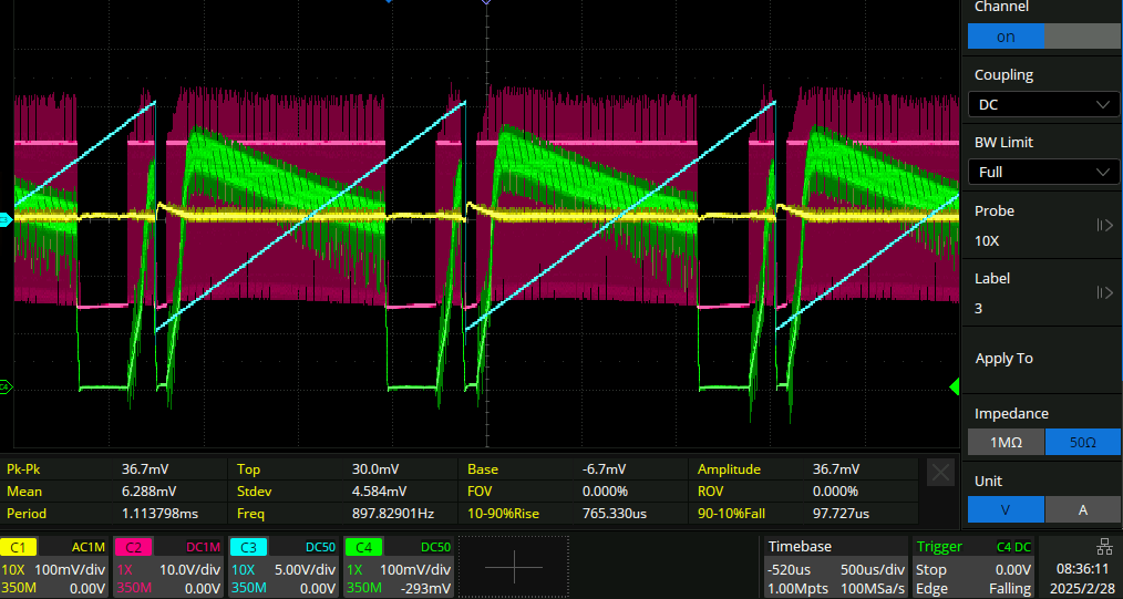
Can’t really say that anything jumps out as bad here, really.
This is the equation for the minimum amount of current from above. The minimum current is not a function of the load, apparently. That seems kind of sus. But the equation for the peak current does have the average load in it, so that makes sense.
In this experiment by the way the supply can only keep working for 10s or so before something heats up enough and the 2A supply limit on my bench supply is reached so the supply voltage collapses.
Anyway clearly the minimum current in the inductor is a huge function of the load on the system since it’s so high when the output ramp is negative.
Left turn
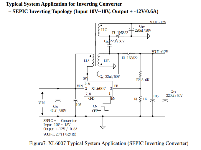
I’m giving up on this. Too much effort. I found the XL6007 on aliexpress, it seems to be a good chip. There are +/-15V modules available on aliexpress for $3.40, so I will buy the module and either plop it in or copy-paste it into my design. Interestingly this represents the first time that I have found a chinese IC that will do my job and no western ones. Also interestingly the datasheet suggests using a transformer for the dual output:
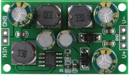
But the aliexpress picture just shows a bunch of regular inductors:
So I am interested to see how it works. For now I’ll hook up the bench supplies and continue load testing.
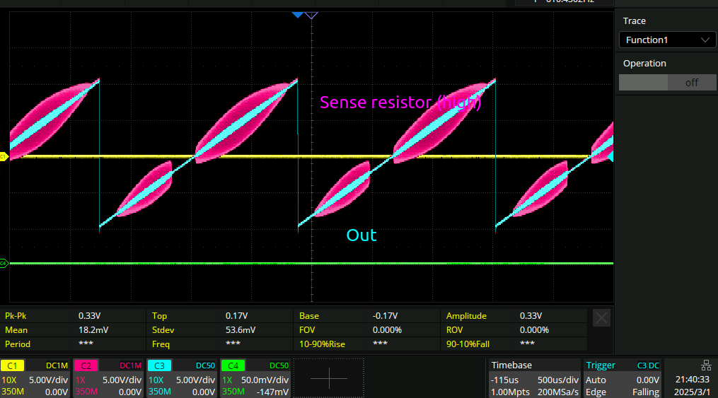
Current limiting
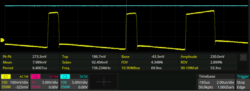
During the course of my load testing I decided to solder a 10R resistor to ground on the output of the AWG. I did this when it was switched on, thinking that the current limiting circuit would work. Reader, it did not. After replacing the op-amp and a bunch of the transistors, I got it back up and running. Then I decided to monitor the current going through the sense resistor, like so:
Interestingly, it seems the capacitance of the cable is enough to set up some oscillation: