Obligatory inversion
Bandwidth
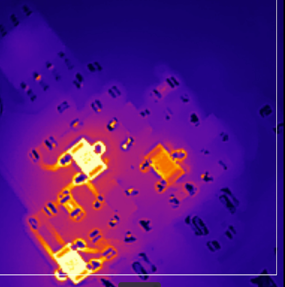
High temps
When the input to the booster stage goes high, the two non-power transistors of the low side get really hot. Like >100deg with a 5V power rail:
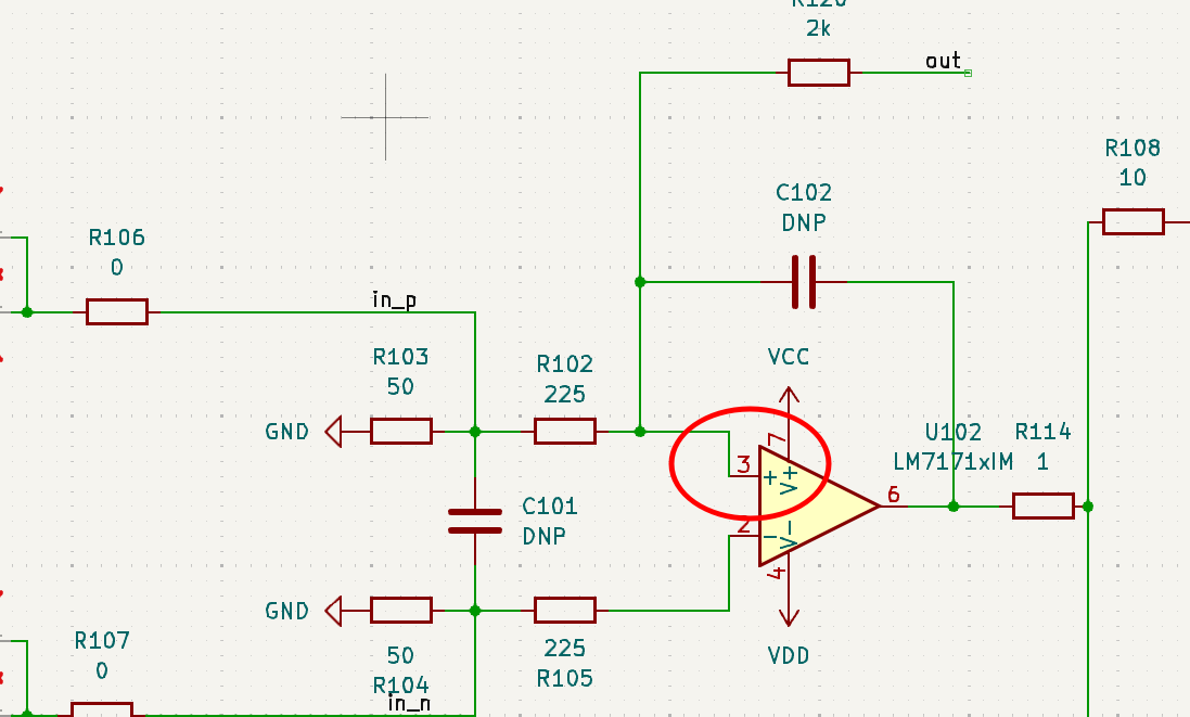
Current path
From probing across the various resistors this is where the current is going I think:
Some measurements:
- R111: 7.7mV → 0.00077A
- R115: 5.6V → 0.016A
- R112: 1.251V → 0.0125A
- R113: 0.124V → 0.124A
- out: 270mA (from multimeter)
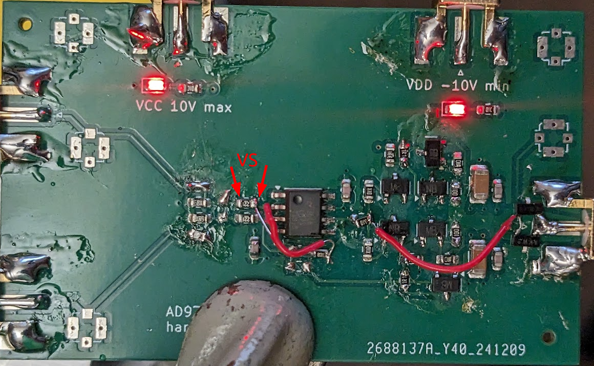
Based on the above and the thermal camera pics it sure looks like a bunch of current is going through Q107 and Q105. So I replaced R116, R117 with 1R. R117 has 0.2V across it. Gottem!
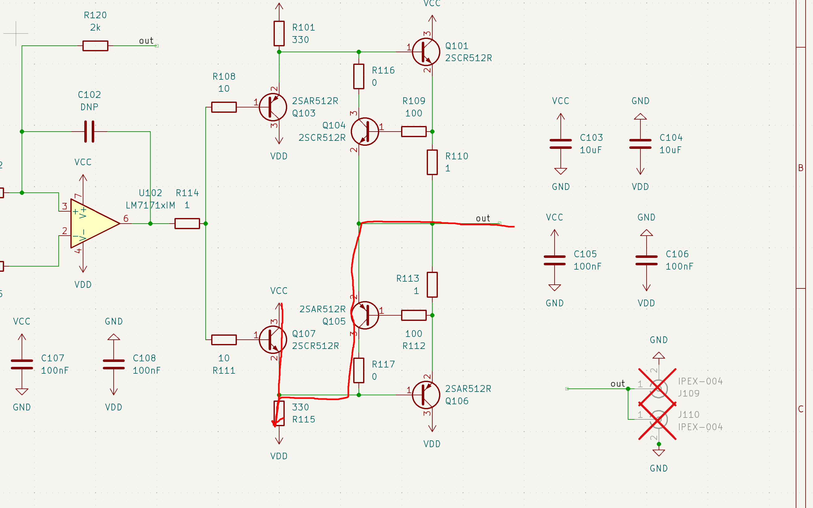
I Added in the two diodes to the output of the amplifier from here and that seems to have fixed the problem, Q107 and Q105 now are no longer super hot with a 5V supply. For some reason I decided not to put them in before, thinking they were unnecessary. That was silly. The transistors can now go to the full +/-10V rails without overheating too much.
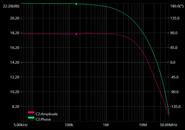
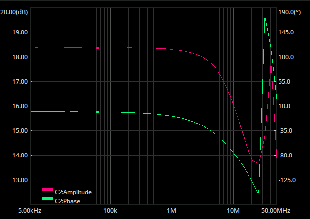
This is what the bode plot looks like now:
Which is a bit worse than before I think. Also the gain is twice as high for some reason.
Bandwidth → current limit constraint.
The fix from before, adding the diodes in, now adds a new path from the output of the op-amp to ground:
Since R114 is 1R, this means that potentially the output of the op-amp goes directly to ground.
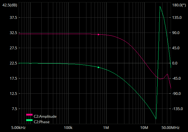
Bandwidth of op amp
As can be seen above the bandwidth of the system is pretty garbage. Here is the op amp by itself:
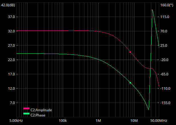
Simulation
Here is what the simulation said it would be from before.
The circuit for the op amp by itself:
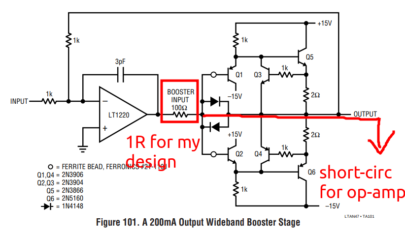
Booster stage:
The booster stage by itself looks like this:
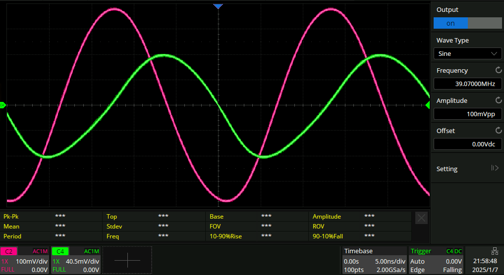
Goes out past 10MHz no problem, but that’s a little spicy at 32MHz!
Here is what it looks like in the time domain:
And when I turn off the waveform generator entirely:
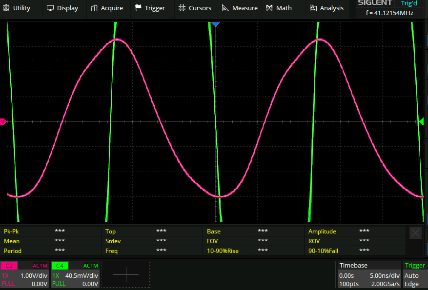
…Note the change in the Y axis scale between the two pics. There does indeed seem to be an oscillator hiding in the circuit. There was something in this in the app note:
So that’s something to keep in mind if it shows up in the full system.
Back to op amp
Here is what the data sheet has to say on the gain-bandwidth product of the amplifier:
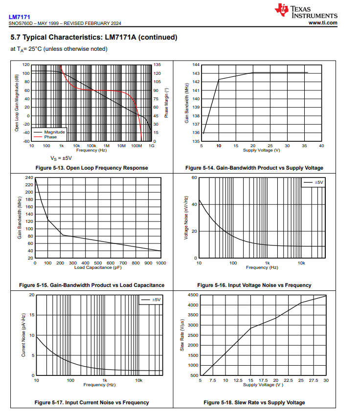
I am using a +/-10 (so 20V) supply, apparently the gain bandwidth produce is 140MHz. I have a gain of
Here is the input capacitance for the 2SAR512R transistors I am using:
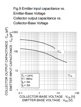
That’s huge! These are regular bipolar transistors! I thought this would be <10pF for some reason. Regardless though I don’t think that this really explains my observations, because above the bandwidth of the op amp by itself was also abysmal, and it wasn’t connected to the capacitive load of two transistors there.
Cable capacitance loading
Maybe the capacitance of the 1m SMA cable going to the scope is loading stuff down somehow.
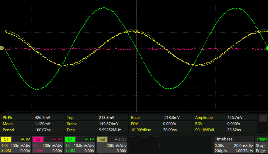
The reference trace (just visible on top of ch1) is the output of the op amp with the cable attached. Channel 1 is with the cable detached. So it’s not that, then.
Lower gain → Higher bandwidth?
1k feedback resistor:
?????? What’s going on here? why does the gain go up after 10MHz? It should be just a bit better than here! Why does it look kind of like the booster stage? The booster stage isn’t connected to the circuit!
Here it is after disconnecting the extra 2k resistor (so back to a single 2k feedback resistor):
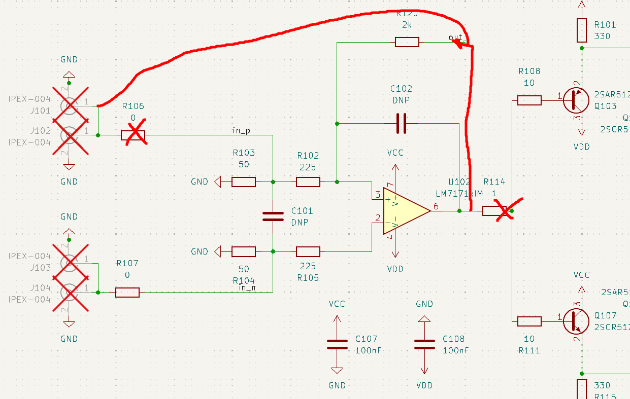
So something was soldered wrong before?
… Yep I think it was soldered to the wrong side of the 200R resistor R102. Should have payed closer attention to the gain.
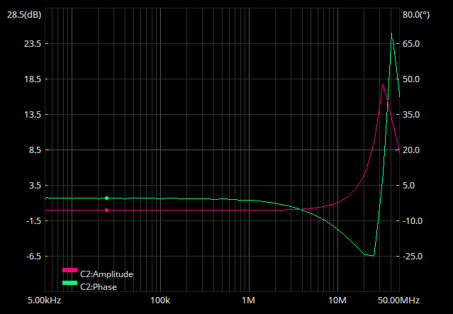
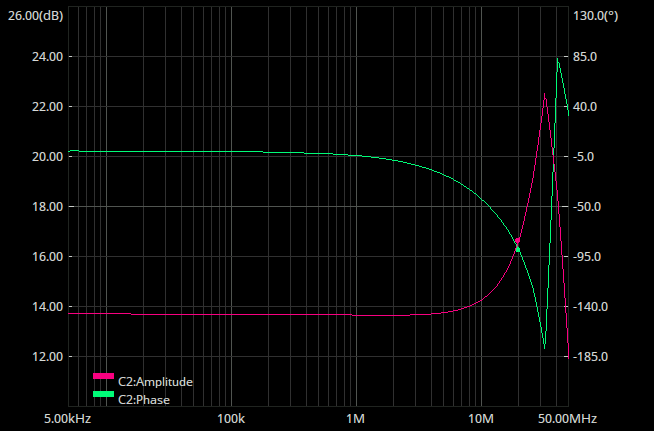
Getting rid of the gain peak
Here is the whole system as-is with no capacitor across the feedback resistor:

There is some pretty huge gain peaking going on at 40MHz.
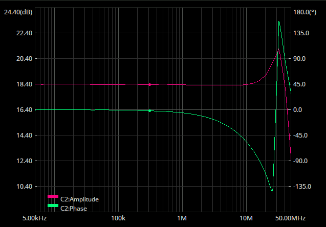
And with a 2.5pF cap added in:
That is about as small of a cap as it’s safe to add I think. The gain is already knocked down by 1dB at 10MHz by this. Since the gain peaking at the end is below the original 18dB gain of the amp I feel that’s enough.
Output swing
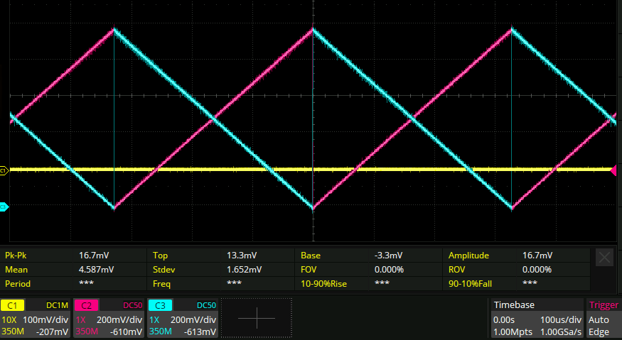
Here is the output from the ad9744 ramping from min to max:
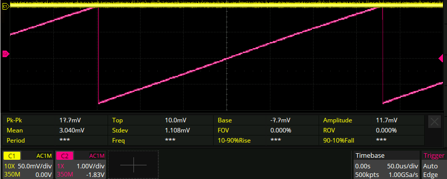 A mere +/-2V. Pathetic! It needs to be +/-10V, so we can burn out the 50R resistors on everyone’s scope. It has a 1.25V compliance range, and 20mA max output. So I should use a 62.5R resistor, but put a 50R one on. That doesn’t explain a factor of 5 difference though.
The signal on top of the 50R resistor R103/R104 is only +/-100mV though, or 0.1/50 = 2mA. So either I’m not sending the right values to the dac, or the output current is not being set correctly.
A mere +/-2V. Pathetic! It needs to be +/-10V, so we can burn out the 50R resistors on everyone’s scope. It has a 1.25V compliance range, and 20mA max output. So I should use a 62.5R resistor, but put a 50R one on. That doesn’t explain a factor of 5 difference though.
The signal on top of the 50R resistor R103/R104 is only +/-100mV though, or 0.1/50 = 2mA. So either I’m not sending the right values to the dac, or the output current is not being set correctly.
The datasheet says this:
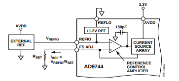

so we should aim for an output current of 0.02/32. 1.2/(0.02/32) = 1920R, which makes sense as all the example resistors in the datasheet schematics have a 2kR value, and that’s what I put in:

Indeed checking the physical board the resistor is 2kR. The voltage across it though was only 0.7V, which isn’t right.
…apparently I powered the chip through some 120R resistors, reducing the supply voltage to 2.2V. I’m a bit surprised it worked at all.
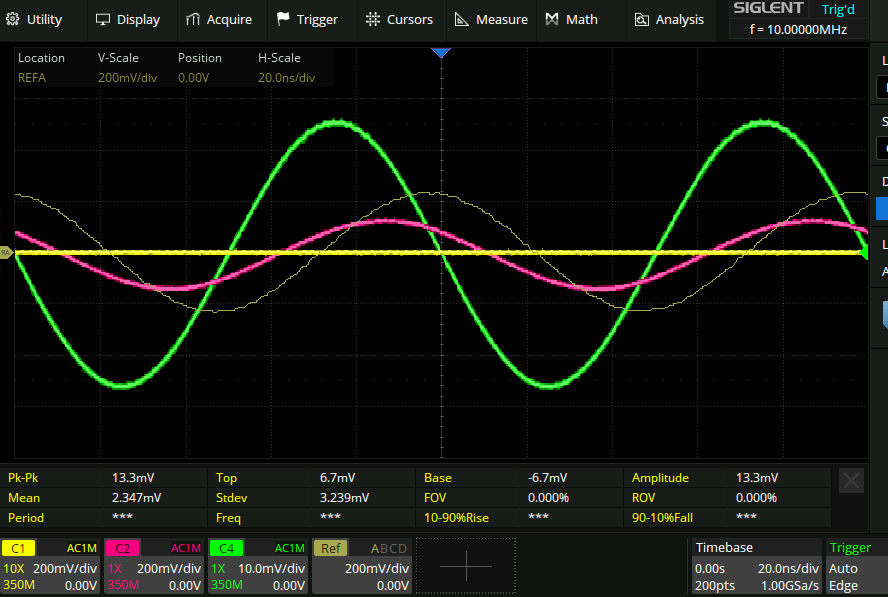
This is what the output look like now, going directly into my scope (so no op amp nonlinearity stuff):
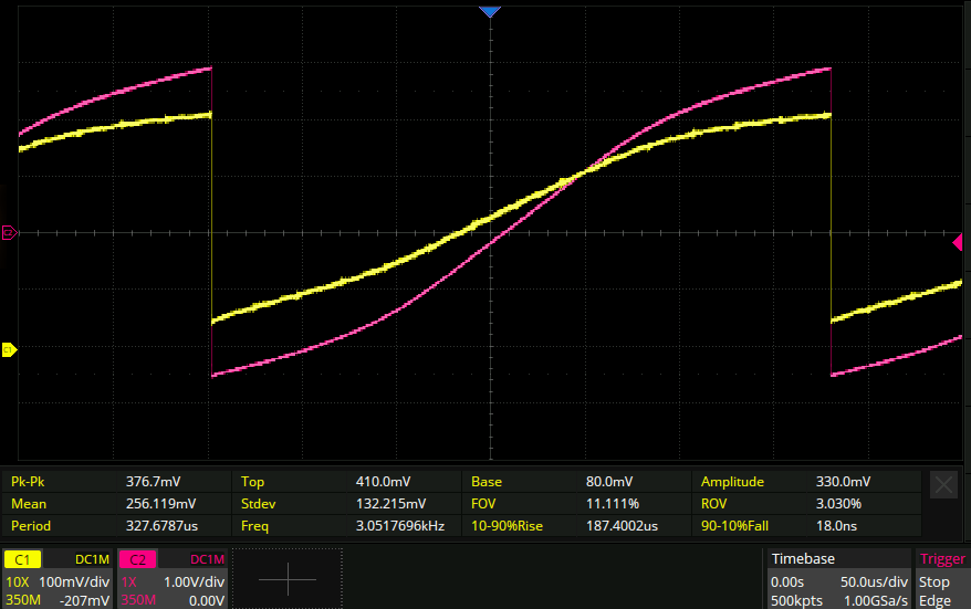
…Not remotely linear, and still too low amplitude!
The only thing left on the output of my circuit was my “ESD” protection circuit:
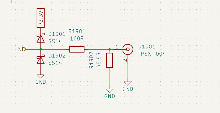
After blowing that off I get this:
Much more sensible, and goes much closer to a proper output voltage!
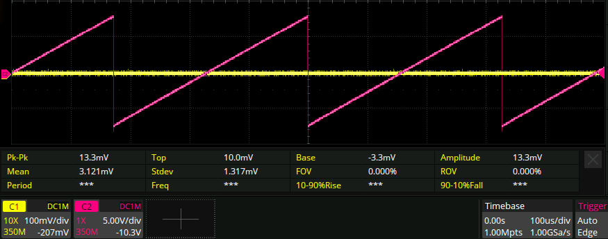
And now, 15Vpp