The awg is sort of vaguely functional in that it produces waves. But, there are a bunch of things left to do. Checklist time!
- Get output impedance of awg to be very low.
- Measure linearity with the scope with and without load
- Fix current limiting behavior such that the AWG can’t blow itself up.
- Send out PCB for split rail power supplies.
- Add barrel jack for external power since USB isn’t going to be close to enough.
- Add USB C?
- input protection for the triggers and digital outputs
- Add library support for the two digital outputs alongside the DAC
- switchable 0R/50R/1k?R termination what for not popping devices under test.
Output impedance
This seems the first order of business. Once this is done hopefully getting the output swing to +/-10V rather than +/-8V is a small gain change. I noticed that the output amplitude dropped quite a lot in response to a 50R load.
…Well it appears I just forgot that my 50R terminator was actually a 20dB attenuator. Here is what the (small signal) swing looks like with and without 50 ohm termination:
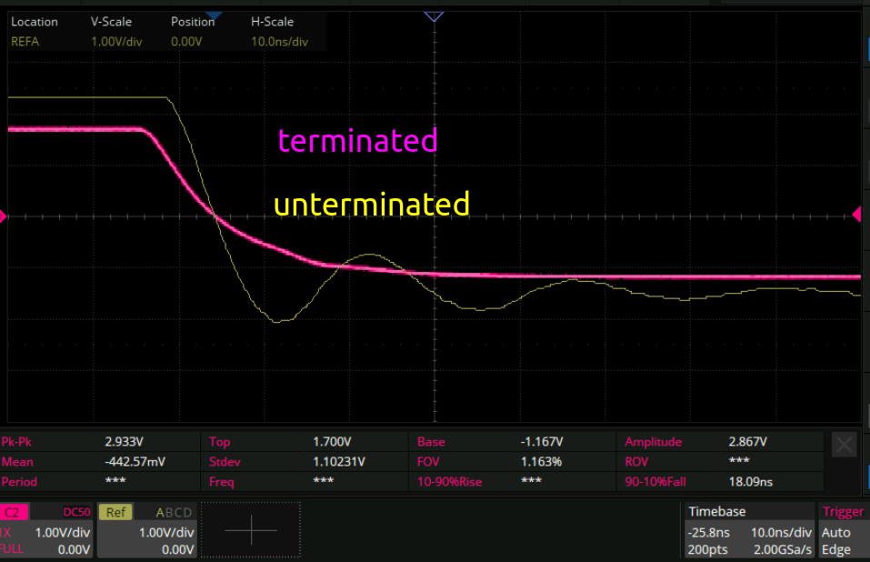
There’s a bit of an amplitude drop there, but is it really so bad?
Large signal swings
Now let’s look at what happens to the signal when the max output swing is applied:
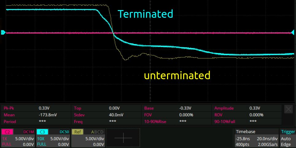
Well it doesn’t look very nice, but terminated/unterminated is not that different.
Negative supply rail
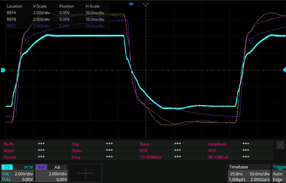
Swinging to -8V or so is quite close to the -10V rail and the op amp is specified up to +/-15V rails. Here is a comparison of -10 to -15V:
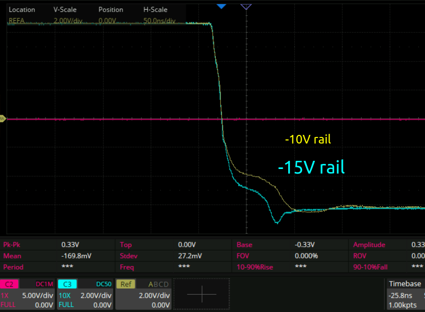
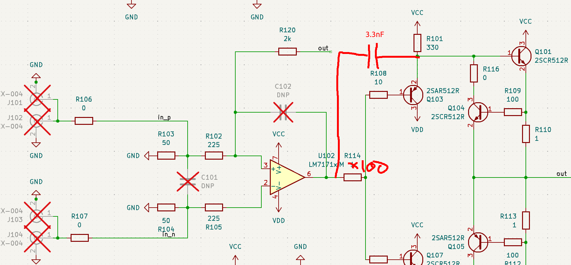
So indeed the -15V looks a bit better, but the ‘hump’ is still present at the end. Also the biasing transistors for Q103 and Q107 get to like 130C with the -15V rail, so I really need to make those bigger. Let’s test that next since that is likely to affect the bandwidth. Let’s try doubling them to 680R and see what happens.
- REFA: Baseline, 330R bias resistor
- REFB: 680R resistor. This “only” gets to 90C when I crank the negative supply to -15V
- REFC: on a whim I detached the feedback diodes I attached earlier. More evidence they are important!
- CH3 blue: 1.2k bias resistors with a +/-15V supply
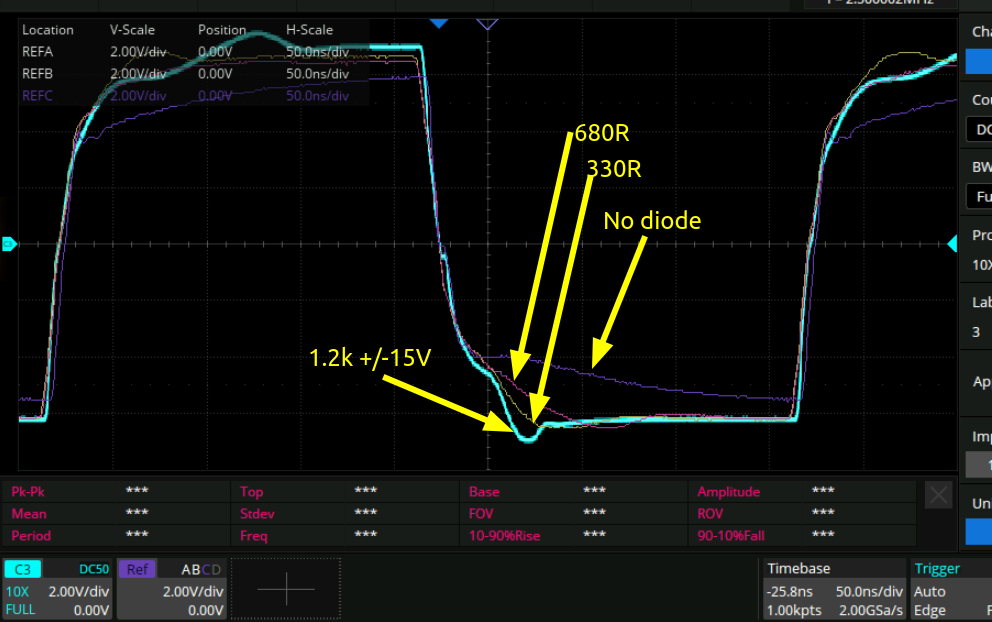
It looks like the 1.2k bias with the +/-15V supply is the winner. I was hoping to get away with a bit less of a supply, since this increases the dissipation in the transistors when there’s an actual load but oh well. Wait no actually those were 2k resistors that were in the 1.2k slot of my resistor book somehow! Anyway this seems to have done a good job on Q103/Q107, they now sit at a gentle 60C or so which I think is more than acceptable. The actual op amp on the other hand is at a rather more toasty 90C. I wonder if we can reduce that by increasing the value of the resistor directly on the output of the op amp R114:
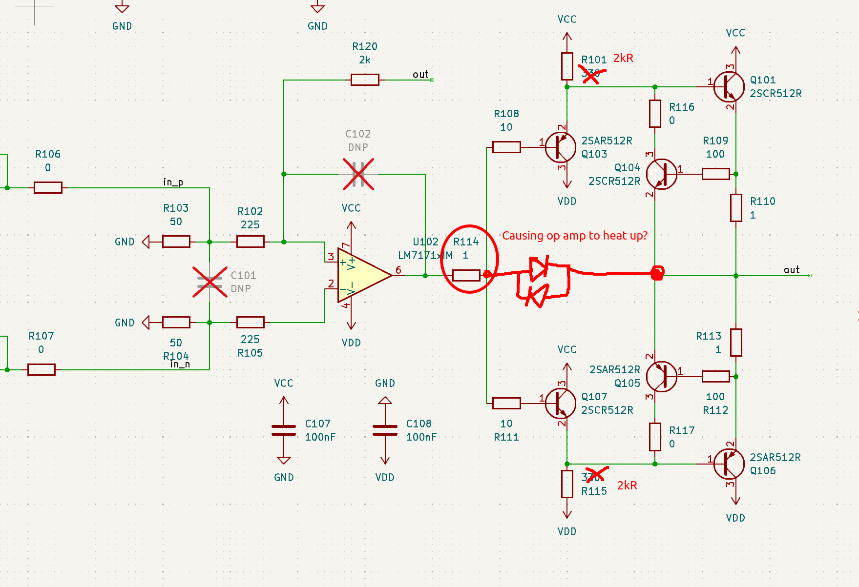
The reason I took it down to 1R before was because it dramatically decreased the bandwidth of the overall circuit. So let’s increase it back up to 100R like the app note originally suggested, and see how that works out:
This seems to have only a slightly lower bandwidth, and indeed the temperature of the op amp dropped to about 60 degrees. But the curious thing is that the output amplitude for the 50R terminated output dropped a lot (pictured) whereas the unloaded output is the same amplitude, +/-7.5V. I don’t know why that would be. Theoretically the actual output of the whole amplifier is still going back to the noninverting input of the op amp, so that should be the error that’s amplified.
I initially thought that perhaps the op amp was hitting the rail somehow, perhaps because of some nonlinear shenanigans involving the diodes connected between R114 and the output. But, that isn’t the case. Wiggling the power supply rails does not change the output much. And this is the actual direct output of of the op amp probed:
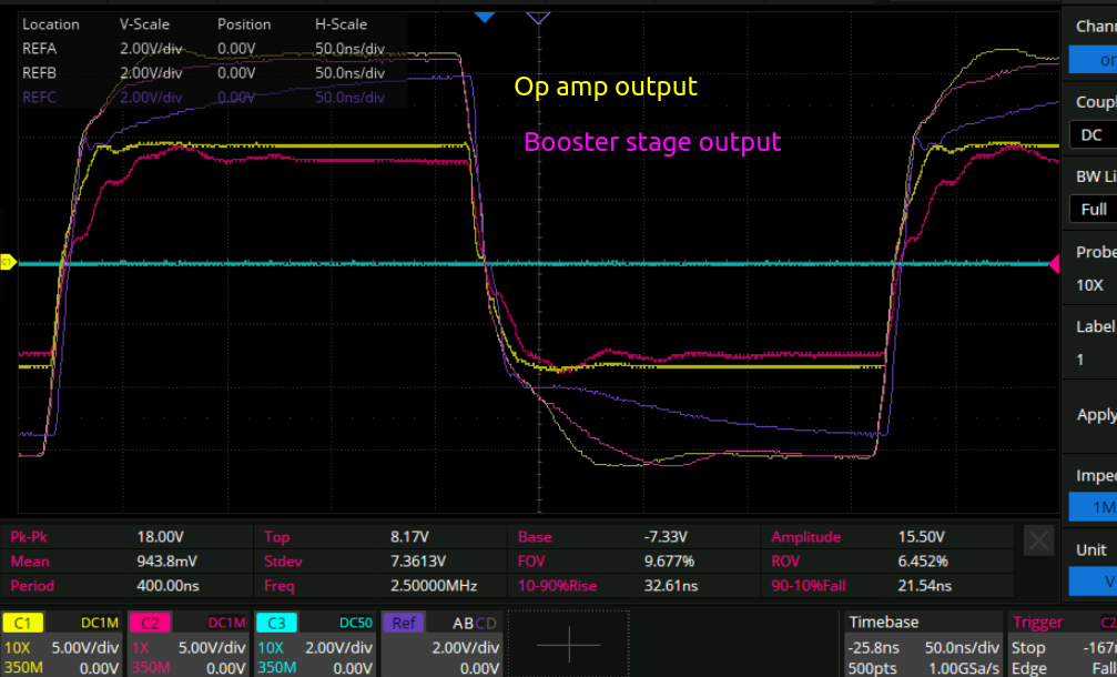
So that’s not the case. This also gives the good and unsurprising piece of information that the wigglyness in the rising and falling edges of the output is due to the booster stage and not the op amp.
… It transpires that I had indeed soldered the feedback resistor such that the op amp did not include the booster stage in its feedback path. This explains rather well the drop in output amplitude when loaded, and also rather calls into question much of todays measurements. So it goes.
Getting back on track, this is what the output now looks like unterminated (ref) and 50R terminated (CH3 blue):
They now indeed are the same amplitude, which is nice, but also the rise/fall is now pretty cooked.
Here is the inverting and noninverting inputs to the op amp, the output of the op amp, and the output of the booster stage together:
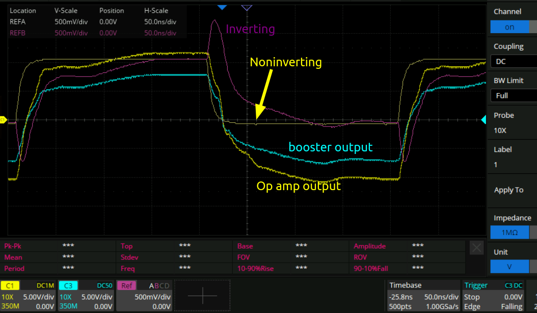
The noninverting input basically is what is coming out from the DAC to the op amp. I don’t really know why the inverting input pulses low and high on the edges of the DAC signal. It looks like some kind of AC coupling type behavior. I don’t know much about dynamic nonidealities of op amps.
Load on the DAC itself
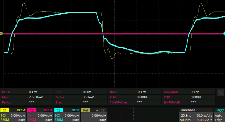
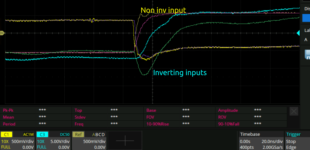
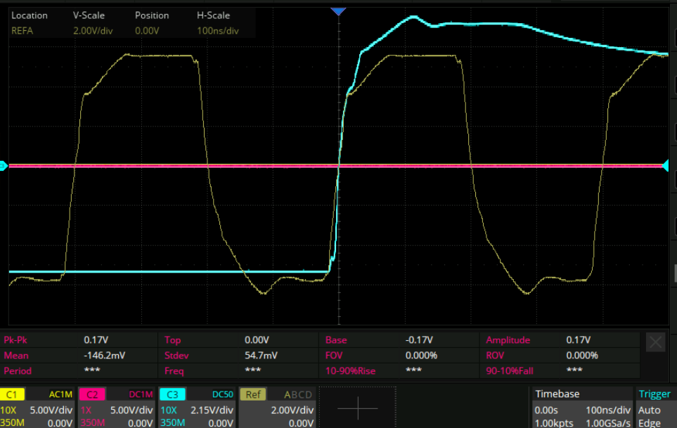
Here is a measurement made across the two input resistors of the op amp:
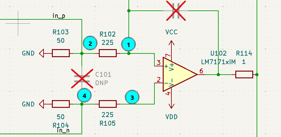
Recall in this paragraph I got the noninverting and inverting inputs the wrong way round on the schematic, as is tradition:
You can see here that on the rising edge of the signal, the noninverting input looks pretty normal. The DAC side of the resistor (4) above has a slightly faster rise time than the op amp side (3). But on the inverting input things are different. There is pretty big undershoot on the inverting input.
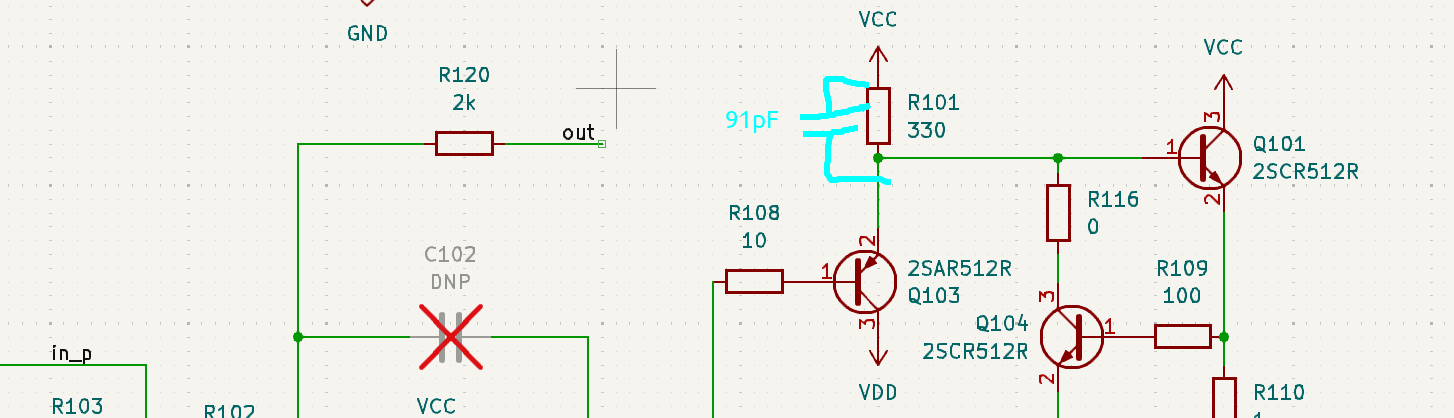
I also at this point changed R114 which seemed to make things better. Now the op amp straight up hits the rail and it’s obvious that the current going through R114 is what’s charging up a bunch of capacitance in the booster circuit. There is some kind of compensation I think that needs to happen here, so that the charging can happen faster.
Some experiments
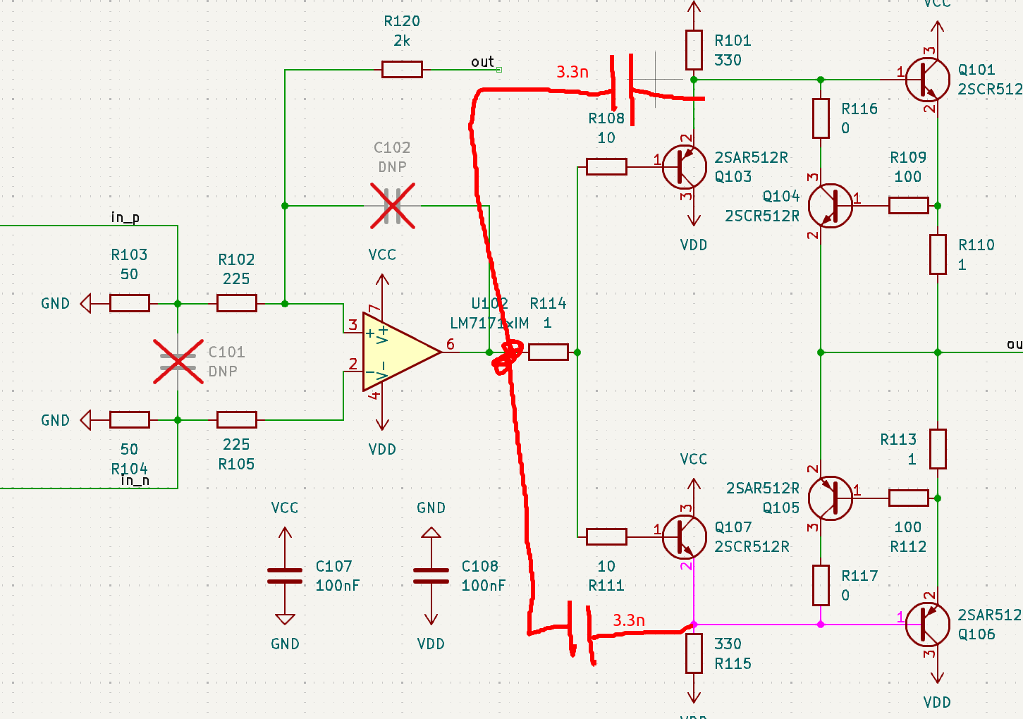
”Speedup” across bias resistor
The very suspicious ramp at the end of the rising edge looks like a capacitor being charged up. I also noticed that touching R101 moved around the location of this ramp, so I added a capacitor to see what would happen. It made it exactly worse, which is good info.
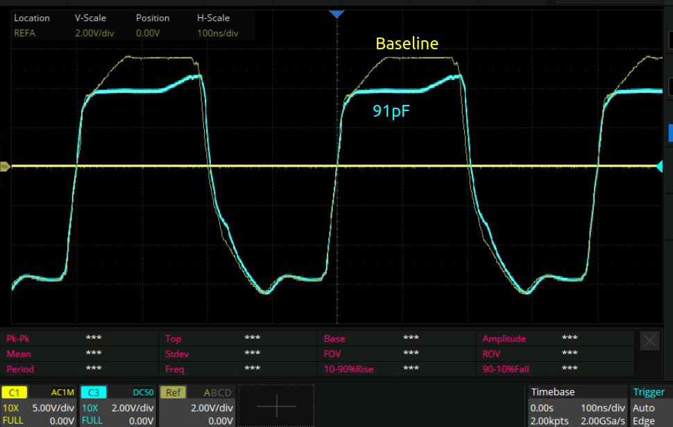
Feed forward across op amp output resistor
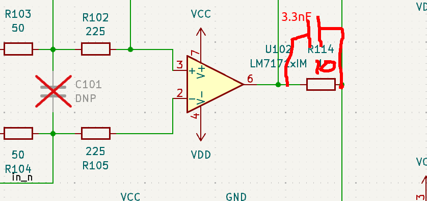
I added 3.3nF since 100pF like before didn’t seem to do anything. I also decreased the frequency of the square wave I’m sending to the AWG. You can see that indeed there is a feedforward behavior. But the frequency of the overshoot is way too low to make up for the ramp at the beginning. And the ramp itself is still very clearly present. If 100pF was way too low, and 3.3nF is way to low frequency (but good enough amplitude) then I am barking up the wrong tree here I think.
Speedup cap across first stage transistor
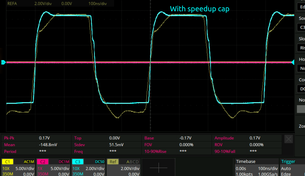
Boom. Now we are talking. Looks like that did the job pretty well. What’s surprising to me though is that the falling edge of the signal is also strongly affected. How can that be?
Two speedup caps
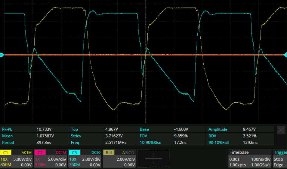
?!?!? Why is it so asymmetric? Here it is zoomed out in time by a factor of 10 (ch3 only):
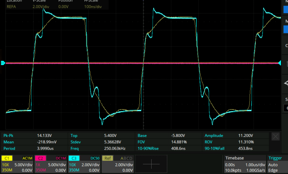
Further confusion: 100pF speedup cap
This is the above redone with a 100pF cap:
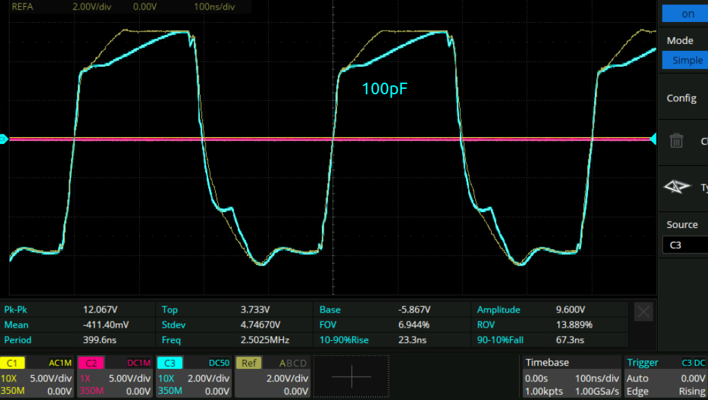
Now it seems again that it’s worse. My confusion has further increased.
PNP transistor replacement.
I then swapped Q107 from a 2SAR512R to a DMMT5401. I did this because the 2SAR512R has this capacitance:
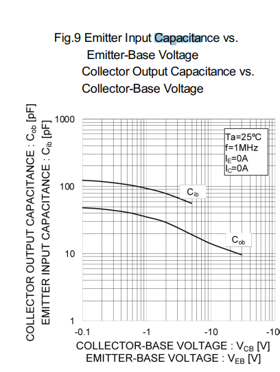
Here “Cob” is apparently the capacitance between the collector and the base. That doc does not define what Cib is. There are so many ways to refer to this it’s incredibly confusing. Why don’t they just say what two terminals the capacitance is measured between? “input capacitance”? Input when your transistor is configured as what kind of amplifier precisely??
Anyway this is what the DMMT5401 has to say on capacitance:
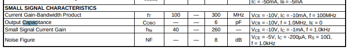
What is Cobo? Is it different from Cob? One presumes not, but how do you know. Anyway the 2SAR512R clearly overall has higher capacitance, so you would think that swapping it out for the lower capacitance DMMT5401 would have a speeding-up effect. This is what it looks like:
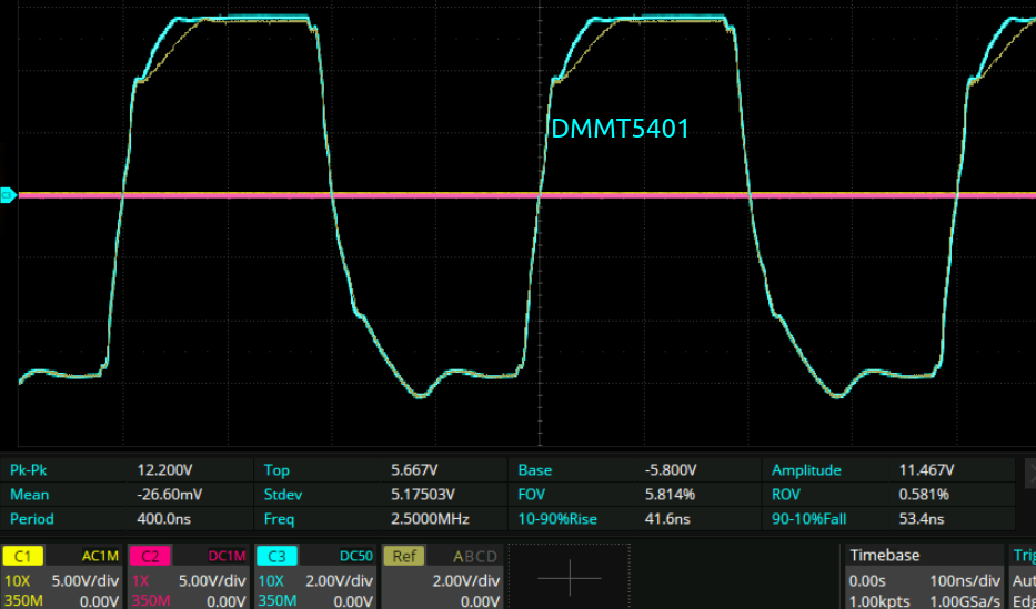
Indeed, this is faster! That’s nice but I doubt that I am going to get a transistor with a 10x lower capacitance even than that, so something else must be possible. I think I’ll just go with 1k of bias resistance via two 2k 0603 resistors to dissipate the power.