AD8606 amplifier
I constructe a noninverting amplifier per the art of electronics basic circuit:
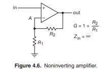
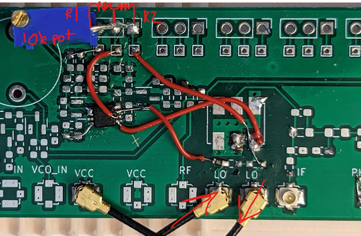
And it looks like this:
Works great. With this amplifier I can get the PLL to lock with a whopping 1.5Vpp input, up from the previous [410mV](^744b71). I think this is satisfactory for the overall design. You can see that the VCO (CH2) is close to its limit:
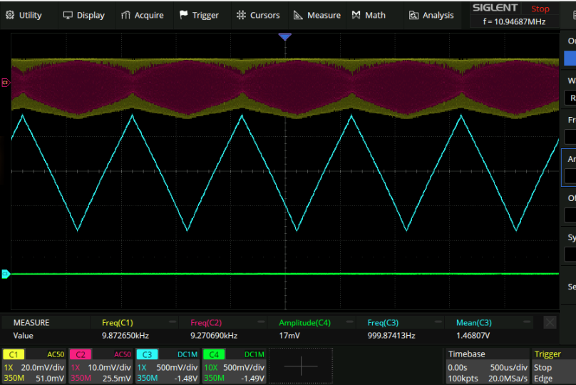
Any higher frequency and it would stop oscillating entirely. CH3 is the input to the VCO. Notice how it requires an offset. The amount of offset required increased with the modulation depth. This seems like it could be to do with maintaining a more constant % modulation.
Performance
~~Here are the performance stats. These were measured with a ramp waveform of amplitude 1.6V:
Input vs output voltage
Over a MHz of swing there - Noice.
Nonlinearity
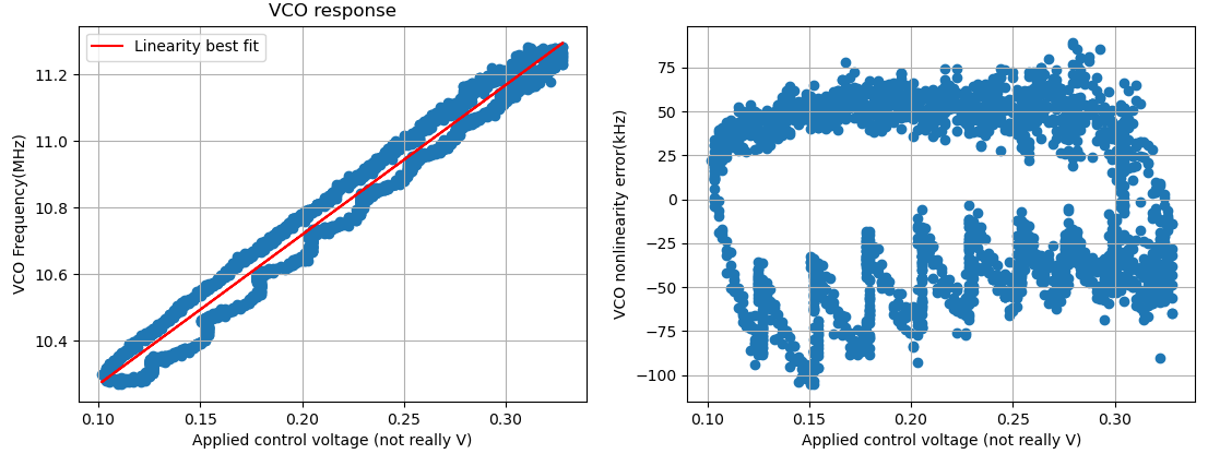
Interesting difference in the response on the ramp up vs ramp down. And the wiggles on the ramp up seem to pretty persistent - you can change the input waveform frequency and amplitude, and get much the same response.~~ Actually all of the above is garbage cause I was not probing the proper input. Whatever, it looks good to me. On to measuring the actual amplifier.
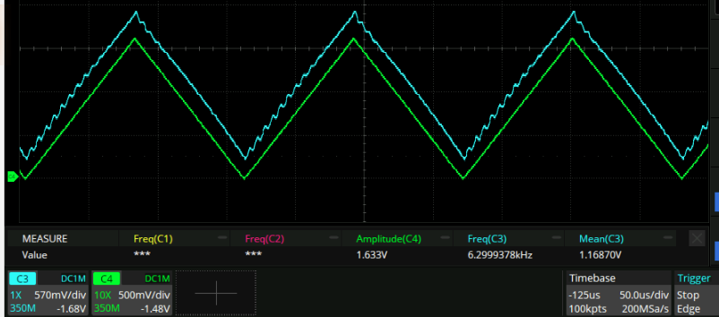
Noninverting amplifier performance
Lovely. So it looks like the closer to the perfect amplifier it is, the better. From previous testing though I know that more gain than this is deleterious.
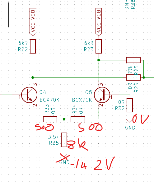
Diff amp performance
Here is the diff amp in its current state:
I have adjusted the voltage of Q5base to be at ground and then adjusted the supply voltage so that the output is centered at ground too. This required a supply voltage of -15V, but we can just decrease the resistor there later and that should be fine.
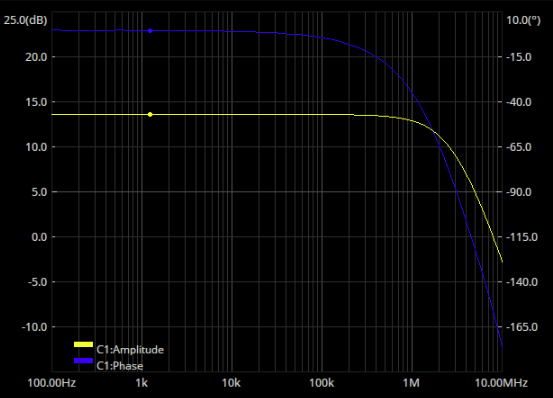
Here is what LT spice says the bandwidth should be of this configuration:
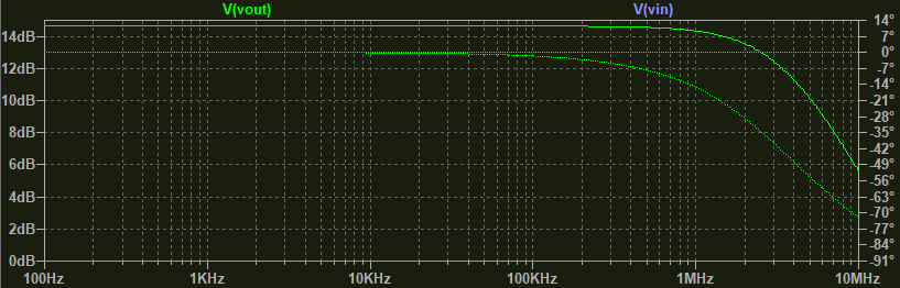
I don’t know what the cause of the difference is. I’ve been abusing these transistors a fair bit but I would be surprised if they were damaged. The output goes straight into the scope - it’s not even loaded down by the VCO. The 3dB bandwidth appears to be about 100KHz, so that wwould imply a capacitive loading of about 265pF, much more than plausibly exists. The only previous result I can find in the notes is this one [here](^a3250d) which also says that the bandwidth should be about 1MHz. Maybe I just need to build another one then.
The parable of the cable
Wow.
REF1 is CH4 before the cable for CH1 was connected. Now that CH1 has been connected CH1 is quite a bit lower in amplitude! This is with my several meter long BNC cable.
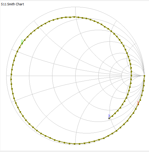
This calls for a VNA capacitance measurement!
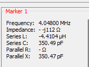
350pF!!! Wow. Now I gotta go measure some other cables! My 1m long SMA cable is still a whole 100pF:
Given that even the small cable is 100pF and the high output impedance of the diff amp (6kR) I think this makes probing the loop with a regular cable a no-go unfortunately.
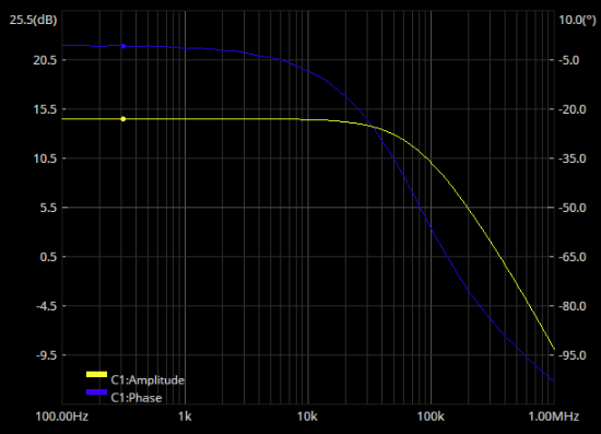
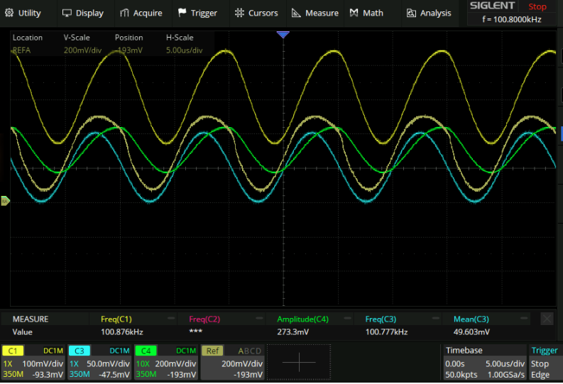
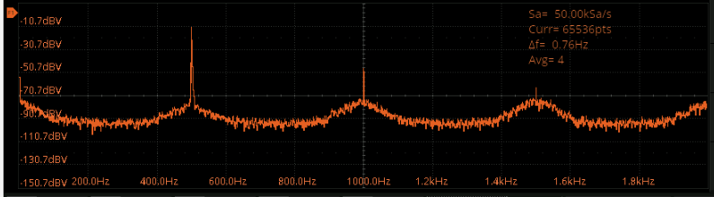
I attached the scope probes with the clippy thing and got this bode plot:
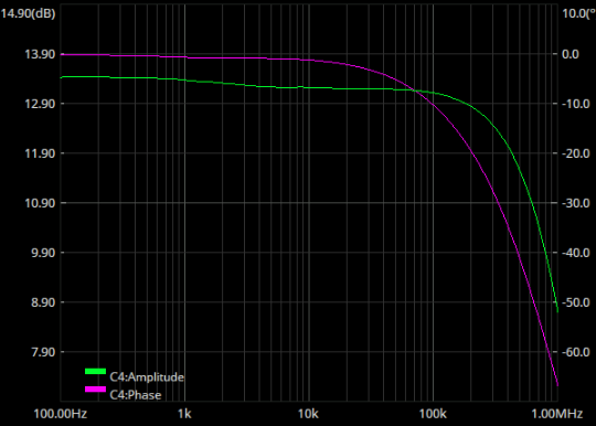
Better, certainly. Good? Questionable. I could reduce the resistor values but the varactor diode doesn’t really need any current to speak of and so this would just waste power when it comes time to plug it into a battery. May as well give it a shot on the real circuit anyway.
PLL performance with diff amp
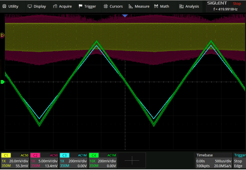
Overall it works pretty well. Locking range is 860mV. Input/output ocillation with maximum modulation in:
Corresponding actual inputs/outputs:
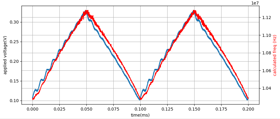
Noice! Here is the above waveform saved and analysed for nonlinearities:
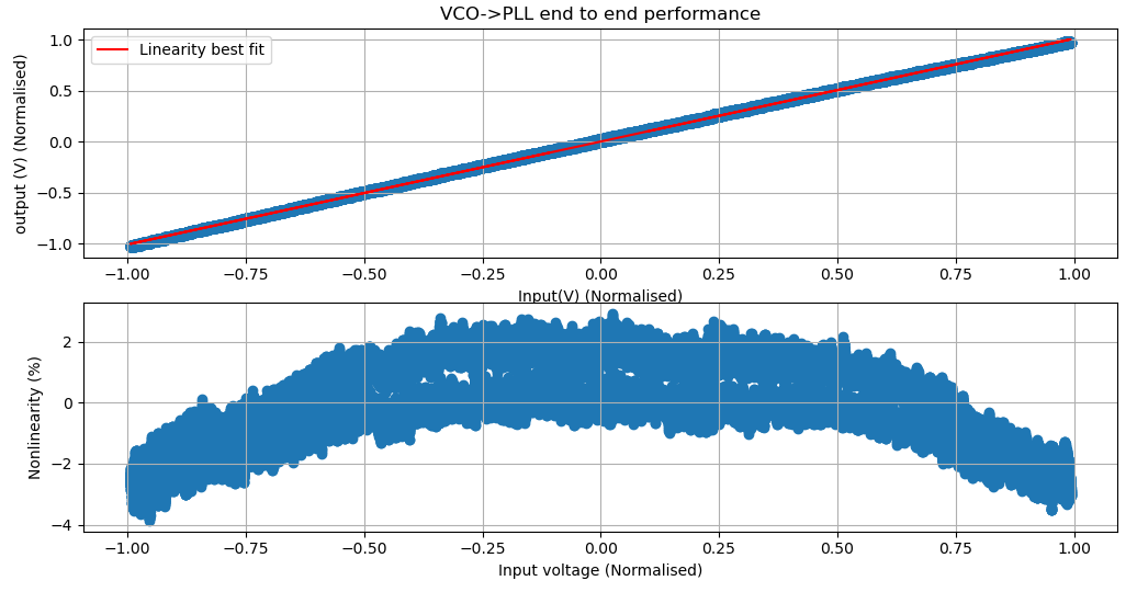
The voltages on the varactor diodes are actually in kind of a different place which might account for some of the nonlinearity here. Here is a 500Hz sine wave with 750mVpp modulation:
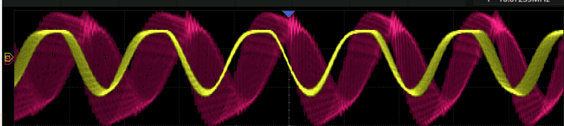
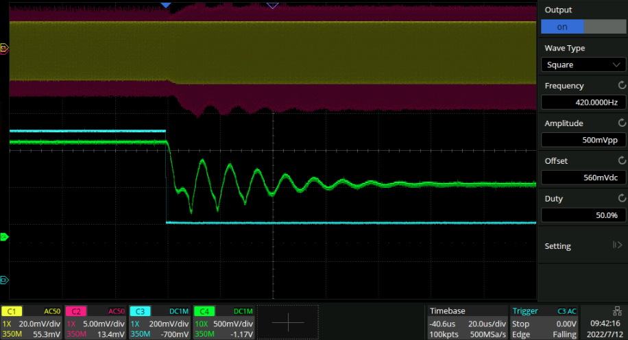
Damping:
Note that when sharp edge are put in the system such as with a square wave the locking range is a fair bit lower, like 500mV instead of 1V. Things are rather underdamped, to say the least:
Maybe we can tune that later but at this point I think that things are working pretty well. Time to whip up a FET input follower so the diff amp isn’t loaded down too much and we should be off to the races.