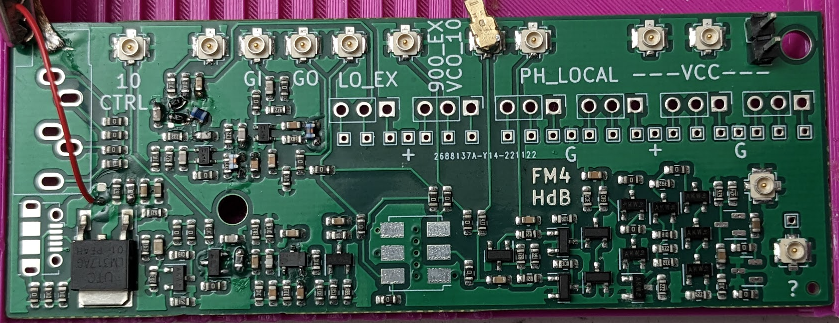
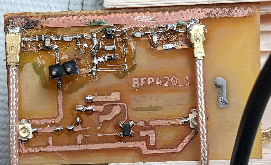
The FM4V pcbs have arrived. This time I used the jlcpcb assembly service. The PCB’s look like this:
The oscillator comes up without any prompting thankfully. The first thing that I want to look at is the 915MHz amplifier. In order not to cook the spectrum analyzer I am going to use the attenuator from 20230115 attenuator.
Assembly problems
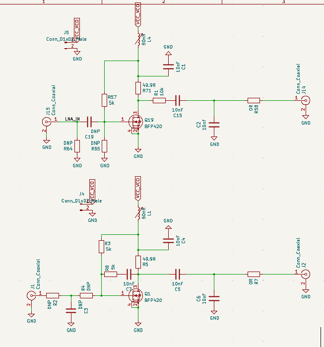
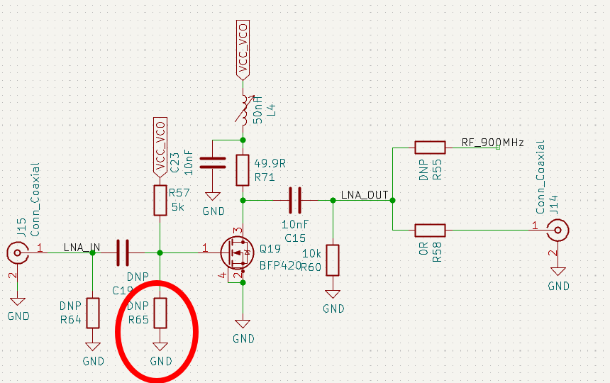 Some dingus soldered a 0R resistor onto R65 which understandably. Once that was removed the amplifier turned itself into a 700MHz oscillator. Nice. Since the VCO is right next to the amplifier I’m going to turn it off by desoldering R53 and then trying again.
That fixed the oscillation, but there is now a bunch of crosstalk coming somewhere from the 10MHz system. The fastest edges there come from the NAND gate, and indeed the interference concides directly with an extremely sharp falling edge there. Disconnecting the phase detector by desoldering R5 gets rid of it entirely.
The amplifier has huge attenuation. Perhaps this has something to do with how someone put a 0R resistor in R64.
Removing that resistor we get this:
Some dingus soldered a 0R resistor onto R65 which understandably. Once that was removed the amplifier turned itself into a 700MHz oscillator. Nice. Since the VCO is right next to the amplifier I’m going to turn it off by desoldering R53 and then trying again.
That fixed the oscillation, but there is now a bunch of crosstalk coming somewhere from the 10MHz system. The fastest edges there come from the NAND gate, and indeed the interference concides directly with an extremely sharp falling edge there. Disconnecting the phase detector by desoldering R5 gets rid of it entirely.
The amplifier has huge attenuation. Perhaps this has something to do with how someone put a 0R resistor in R64.
Removing that resistor we get this:
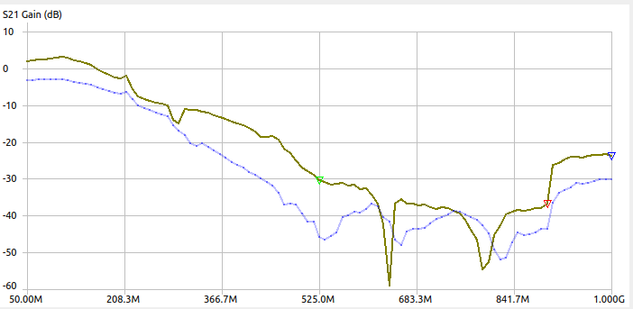
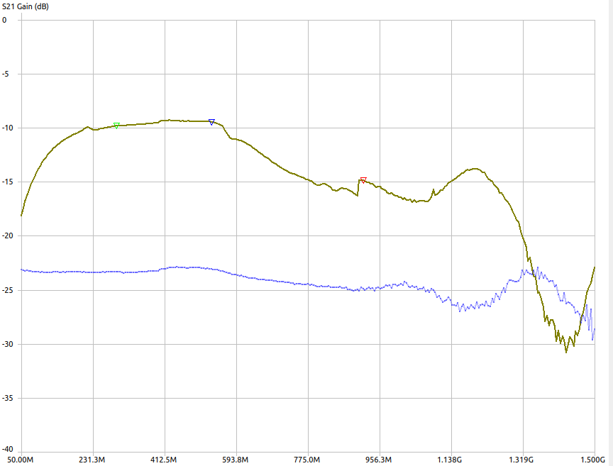 This is with 20dB attenuation from the attenuator, bottom line is ref through a THRU trace on the ufl RF demo kit.
Optimising
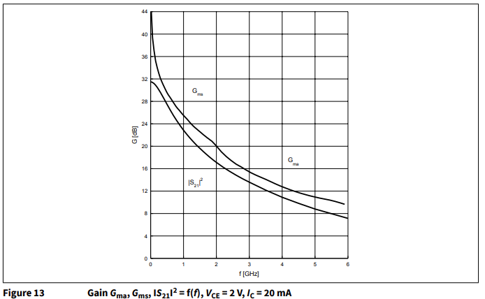
The BFP420 should have way more gain than this though:
So let’s measure some important parameters:
- Vbe = 0.951V
- Ic = 2.79 / 50 = 55mA
- Ib = 3.59 / 4700 = 0.76mA
…This seems like it’s being driven rather hard.
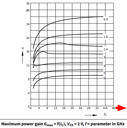 And indeed we seem to have travelled off the end of the x axis. Absolute maximum is 60mA though and transistor doesn’t seem to be too toasty, so we should be still OK.
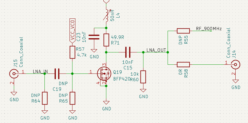
I think I want this amplifier to have a fairly low output impedance so as to be able to drive the mixer nice and hard, and so instead of increasing R71 I will increase R57:
And indeed we seem to have travelled off the end of the x axis. Absolute maximum is 60mA though and transistor doesn’t seem to be too toasty, so we should be still OK.
I think I want this amplifier to have a fairly low output impedance so as to be able to drive the mixer nice and hard, and so instead of increasing R71 I will increase R57:
 I think we want somewhat less than a factor of 10 less bias current, so I’ll go with 33kR.
…aaand the transistor seems to be blown. I resoldered another one, but for future reference the current draw without the transistor attached is 91mA. Since the regulator is a linear one, any deviation from this is the current consumption of the circuit.
I think we want somewhat less than a factor of 10 less bias current, so I’ll go with 33kR.
…aaand the transistor seems to be blown. I resoldered another one, but for future reference the current draw without the transistor attached is 91mA. Since the regulator is a linear one, any deviation from this is the current consumption of the circuit.
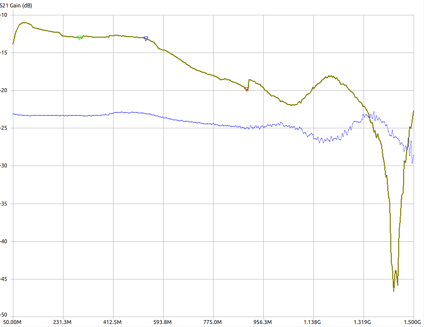
With R57=33k and R71 still 50R the Ic is 11mA, Ib is 3.6 / 33k = 0.1mA. Looks like this was the desired Ic adjustment, but the gain looks like this now:
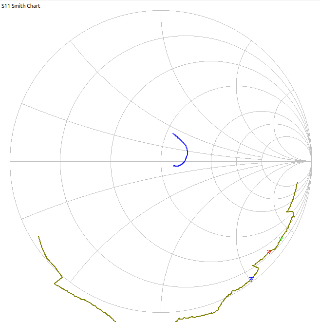
 Which is quite a bit worse. The S11 smith says that the input impedance is 55+j20R. I’m not sure but that sounds pretty close to 50, sufficiently close anyway that the 20dB performance gap is not explained by it.
The application note has a pretty big inductor (about 50R at the target freq) in series with the input for 50R matching though, and I also notice that the input impedance of this thing barely changes with turning the device on and off. Also the app note for ‘high impedance input’ has basically the same circuit as I do, so I think there might be something fishy going on here.
…Measuring the input capacitor, it’s 5pF. I should check the BOM that got sent out cause it sure looks like the JLCPCB people got a lot wrong here. Using a 300pF capacitor gives this input impedance (0-915MHz):
Which is quite a bit worse. The S11 smith says that the input impedance is 55+j20R. I’m not sure but that sounds pretty close to 50, sufficiently close anyway that the 20dB performance gap is not explained by it.
The application note has a pretty big inductor (about 50R at the target freq) in series with the input for 50R matching though, and I also notice that the input impedance of this thing barely changes with turning the device on and off. Also the app note for ‘high impedance input’ has basically the same circuit as I do, so I think there might be something fishy going on here.
…Measuring the input capacitor, it’s 5pF. I should check the BOM that got sent out cause it sure looks like the JLCPCB people got a lot wrong here. Using a 300pF capacitor gives this input impedance (0-915MHz):
 Which looks much more like the application note (high input impedance at 100MHz).
Input matching
I think that I should initially run the system at 300MHz, to be comfortably within the scopes 500MHz bandwidth.
At 300MHz the input inpedance of the amplifier is 0-128jR. ~~~Referring to 50R matching. this means:~~~
Adding in an inductor of ~128R cancels the impedance at 300MHz:
 But that’s not really what I want cause the impedance is wayy too large. Doing the maths in the Hagen textbook I don’t really see how it’s possible to match a purely imaginary impedance to a real 50R system. The imaginary bits just shuffle around. But there is an example in an application note
 So I will try to assemble this and then see what I measure.
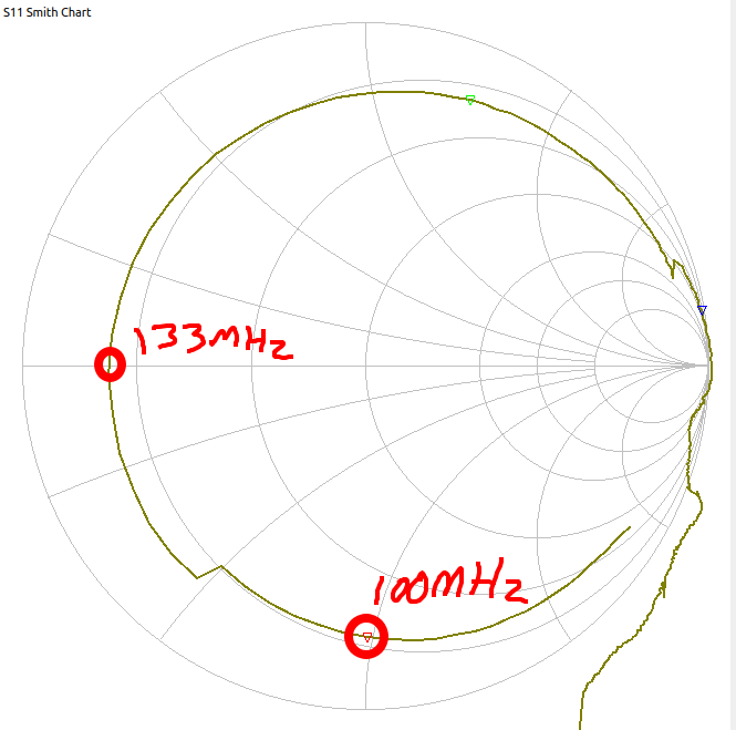
The exact transistor I am using isn’t one of the examples, and the match is supposed to be at 100Mhz. This is what I get:
So I will try to assemble this and then see what I measure.
The exact transistor I am using isn’t one of the examples, and the match is supposed to be at 100Mhz. This is what I get:
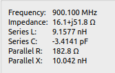
Impedance measurements
 Where the impedance cr
20230415 Back in da game
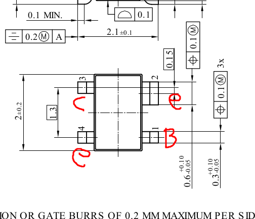
Back debugging things. Kick this off with the pinout of the BFP420, which I have forgotten:
 The datasheet requires way too many layers of indirection to read this imo.
Also the app note makes very little sense:
The datasheet requires way too many layers of indirection to read this imo.
Also the app note makes very little sense:
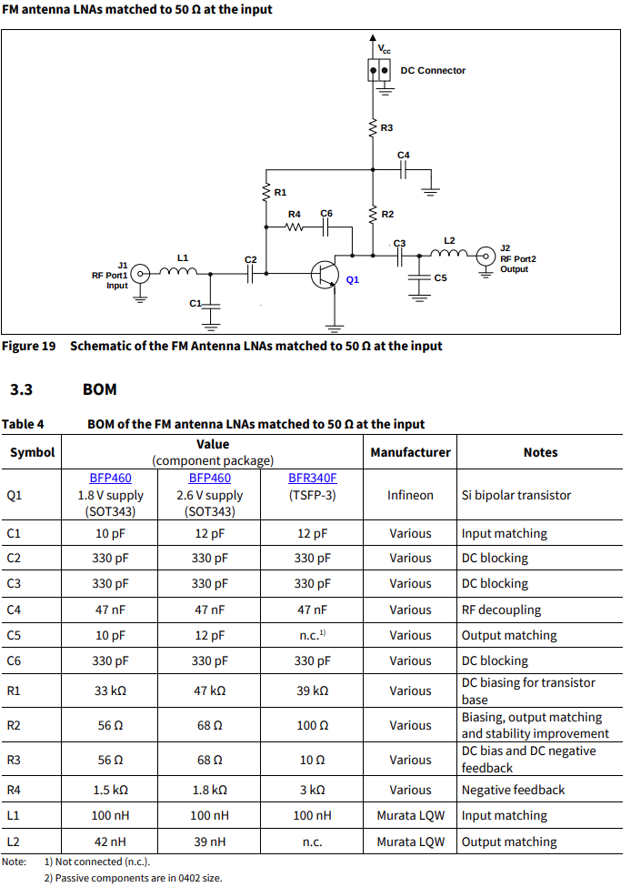
 Since I haven’t actually gotten the amplifier working at all at any point and the example schematics in this app note aren’t quite what I laid out initially I took the opportunity to whip up a pcb:
 That duplicated the schematics in the app note exactly.
Here is the pcb (it got left in the etchant too long):
That duplicated the schematics in the app note exactly.
Here is the pcb (it got left in the etchant too long):
 and here are the results for the 50R matched one (The one with Q1):
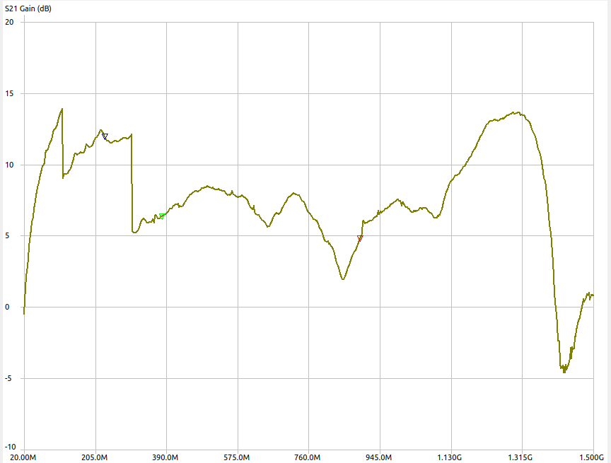
 The gain (+20dB because I put 20dB of attenuation on):
 This looks more or less in line with the app note, which had gains of 15-18dB with different but similar transistors.
Just like the app note the gain seems to increase with increasing vcc too, which is nice. I wonder why that is though.
This looks more or less in line with the app note, which had gains of 15-18dB with different but similar transistors.
Just like the app note the gain seems to increase with increasing vcc too, which is nice. I wonder why that is though.
Impedance measurements (again)
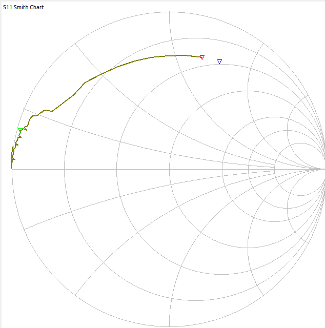
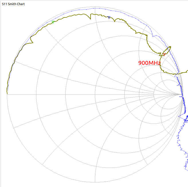
Now that we have a good starting point the time has come to try to get it to work for higher frequencies. The matching looks like this from 50-1000MHz:
 So I think we are all good there. The gain looks like this:
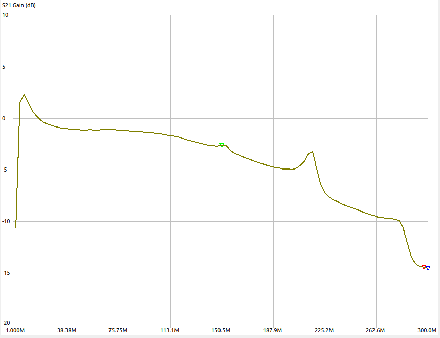
which obviously needs to be changed. Let’s see what happens when we remove the Feedback resistor R4:
 Well that seems to have improved things across the board but not by nearly enough.
A moment of attenuated brain function
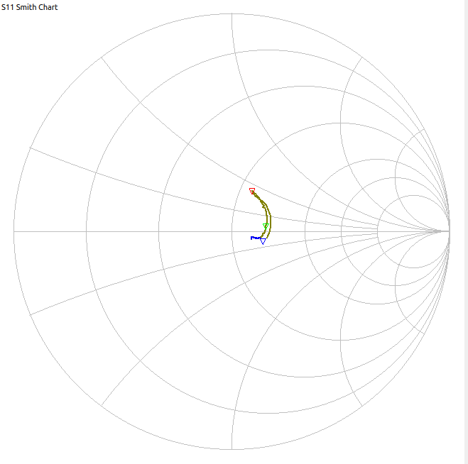
The reason that the matching was so good over the whole frequency range was because the setup went vna→attenuator→amp→vna. I did this because I was avoiding damage but of course this also meant that’s all I measured. Here’s the real input matching:
 Much more in line with what I have come to expect: egregiously bad.
One thing I just noticed in the datasheet is this:
Much more in line with what I have come to expect: egregiously bad.
One thing I just noticed in the datasheet is this:
 My Ic is according to my power supply less than 1mA. So I should bump that up to 10mA. the app note says that it will be 3.5mA and the transistors aren’t that different I would have though so I’m not sure what’s going on here.
Honestly other than providing a design that probably works I’m getting the impression that this app note is BS for the most part. It gives zero information on how to actually do the input impedance matching, for example.
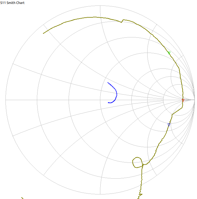
Here is the smith chart for the input to the amplifier with the inductor L1 shorted and the capacitor C1 removed:
My Ic is according to my power supply less than 1mA. So I should bump that up to 10mA. the app note says that it will be 3.5mA and the transistors aren’t that different I would have though so I’m not sure what’s going on here.
Honestly other than providing a design that probably works I’m getting the impression that this app note is BS for the most part. It gives zero information on how to actually do the input impedance matching, for example.
Here is the smith chart for the input to the amplifier with the inductor L1 shorted and the capacitor C1 removed:
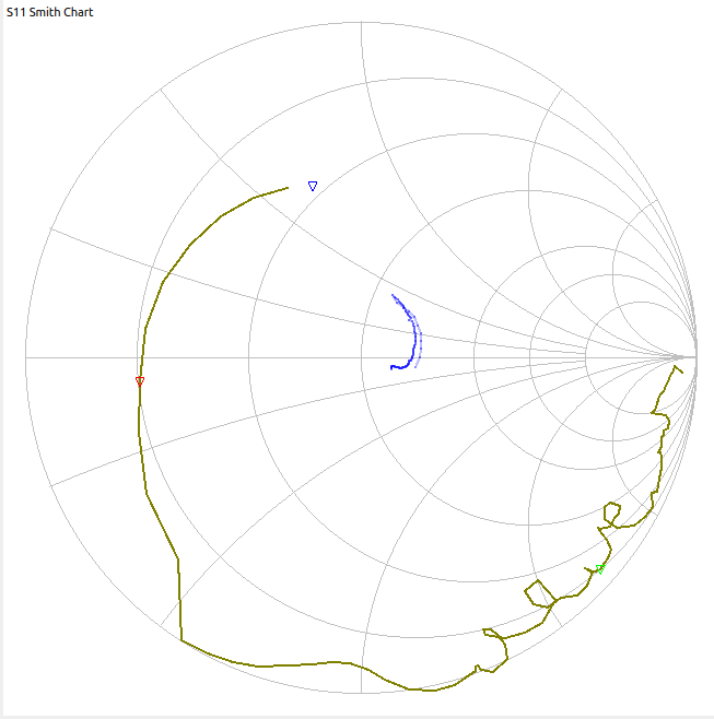 Since C2 is 330pF and DC blocking I think this should be a valid way to measure the input impedance? I don’t really know how to go about doing this, the textbooks don’t really say how you measure an active device like this much.
Attaching components for matching.
Regardless the impedance is 10-j2.6R. So First off I need a 40R inductor. That’s 40/(2pi900e6) = 7nH apparently. Soldering that on did not lead to much of a change. The impedance of this component directly to ground on a separate test board is this:
 interestingly it basically gets the inductance right, but impedance seems to be too low. Looks like I need to roughly double that. ---Record-scratch---
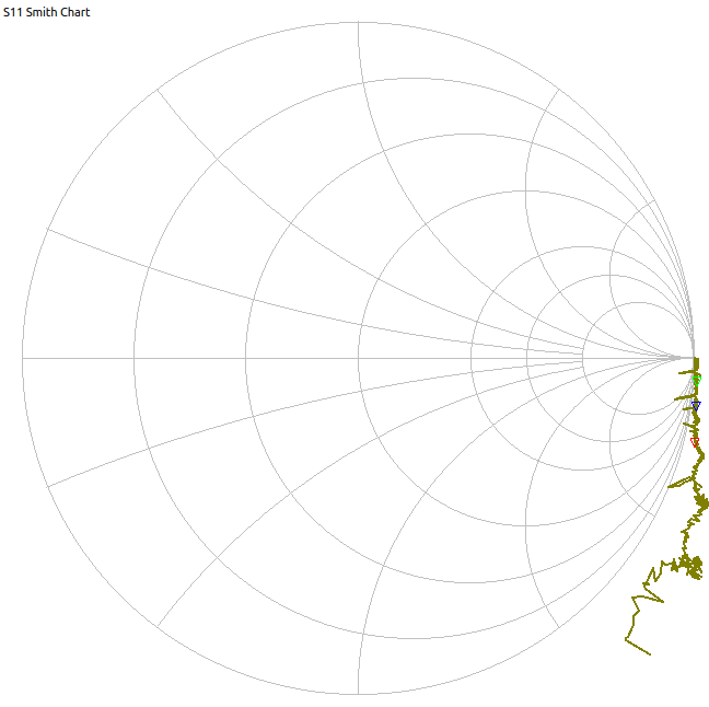
 That’s a dead short to ground looks like my cal is a bit off. After re-calling things stuff looks more sensible. Here is the input to the amplifier now:
That’s… not what I expected.
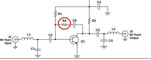
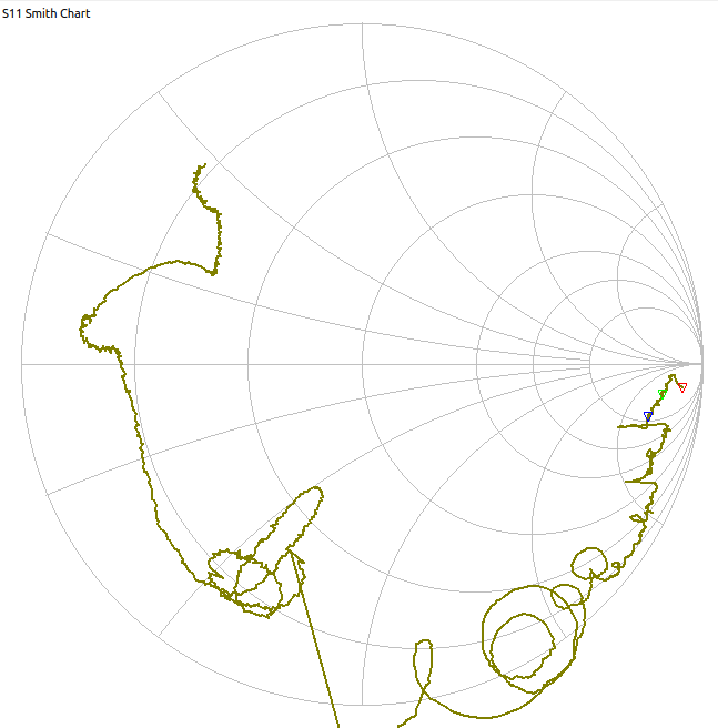
The smith chart changes radically when I put a finger near it. Here is what it changes into when I attach the feedback network of R4 and C6:
 utterly different. The fact that the trace lies outside the smith chart I think is an indication that this is a powered circuit that is adding energy to the system.
—Record scratch++—
Jokes there was a disconnected cap. Here is the real input impedance:
utterly different. The fact that the trace lies outside the smith chart I think is an indication that this is a powered circuit that is adding energy to the system.
—Record scratch++—
Jokes there was a disconnected cap. Here is the real input impedance:
 Much saner.
Some progress.
I found a cool website where you can put in an impedance and see how a smith chart moves it around. I added in my impedance and calculated what would be required to bring it into 50R:
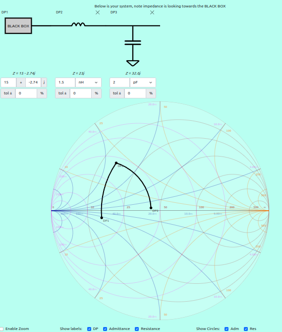 It seems the component sizes required are really small!
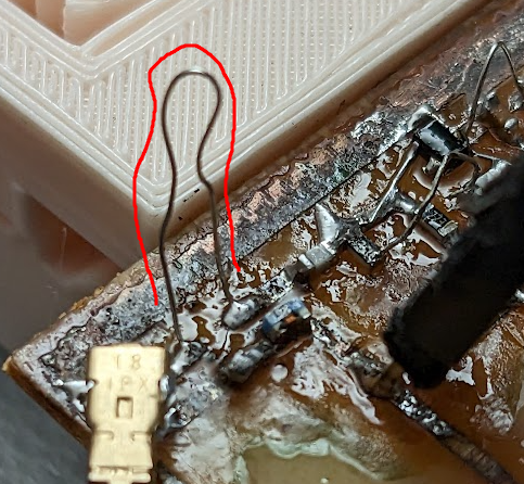
I added just this piece of wire to the circuit:
It seems the component sizes required are really small!
I added just this piece of wire to the circuit:
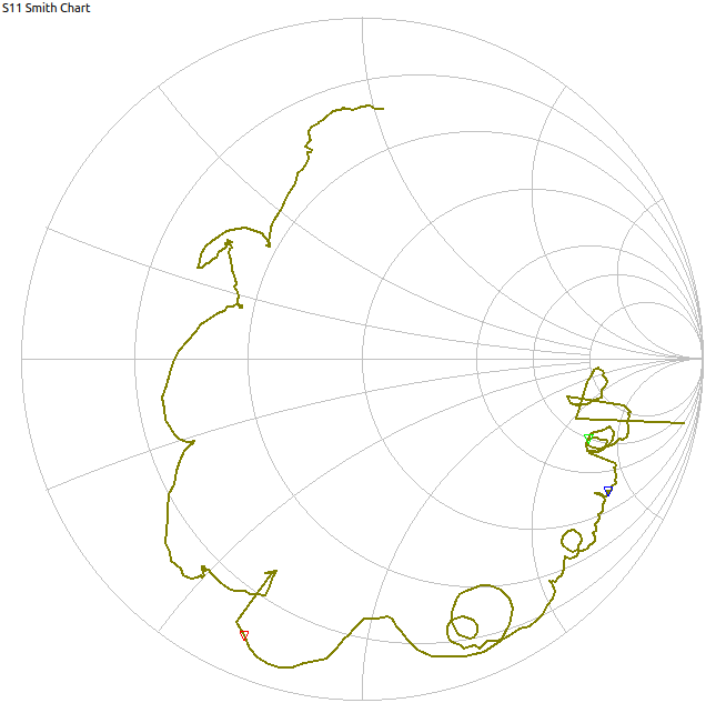
 And it did this to the smith chart!:
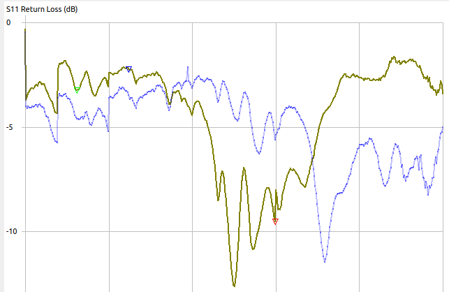
 The S11 return loss now looks like this:
 I think -10dB is really about as good as necessary here; I’ve proved that some amount of matching is possible. Now to test the amplifer performance. This will require a 2 port cal on the vna and also I will need to put the attenuator on the output of the vna to be able to measure the gain properly.
Gain meassurements:
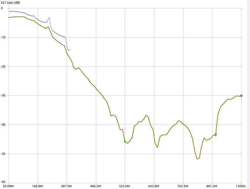
Here is the gain with the same components values as the 100MHz reference design:
 I’m assuming this looks bad from terrible output matching. From a plain no-parasitic no-nonsense reading of the schematic the amplifier should have an output impedance of R2+R3 == 100R ish which doesn’t sound so bad. So I will remove L2 and C5 from the schematic:
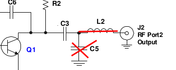 This results in a gain of about 10dB at 900MHz. I added an additional 50R resistor on to the output and it dropped by about 4dB which indicates that in fact the output is in fact fairly well matched at this frequency. If the output impedance was far above 50R then it would drop by a lot, and if it was far below 50R (unlikely!) then it would drop below that. I think maybe I should be looking at the s21 phase at this point but not sure how to use that to come up with a complex output impedance.
Adding loop wires to the output like I did with the input seems to make things quite a bit worse though.
Idea: remove the negative feedback. That seemed to help a tiny bit but not much.
This results in a gain of about 10dB at 900MHz. I added an additional 50R resistor on to the output and it dropped by about 4dB which indicates that in fact the output is in fact fairly well matched at this frequency. If the output impedance was far above 50R then it would drop by a lot, and if it was far below 50R (unlikely!) then it would drop below that. I think maybe I should be looking at the s21 phase at this point but not sure how to use that to come up with a complex output impedance.
Adding loop wires to the output like I did with the input seems to make things quite a bit worse though.
Idea: remove the negative feedback. That seemed to help a tiny bit but not much.
Design guide update
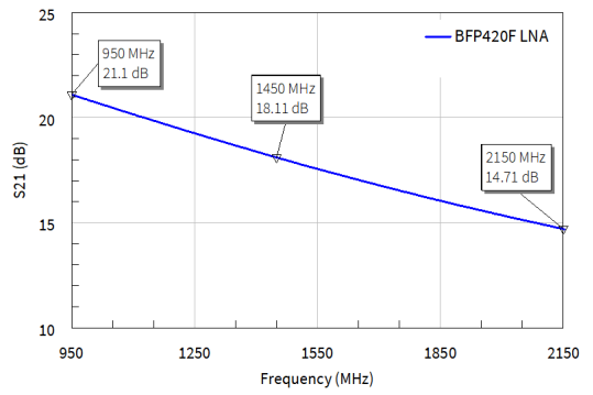
As usual I did not do a proper literature search. Here is a reference circuit for the exact transistor that I had:
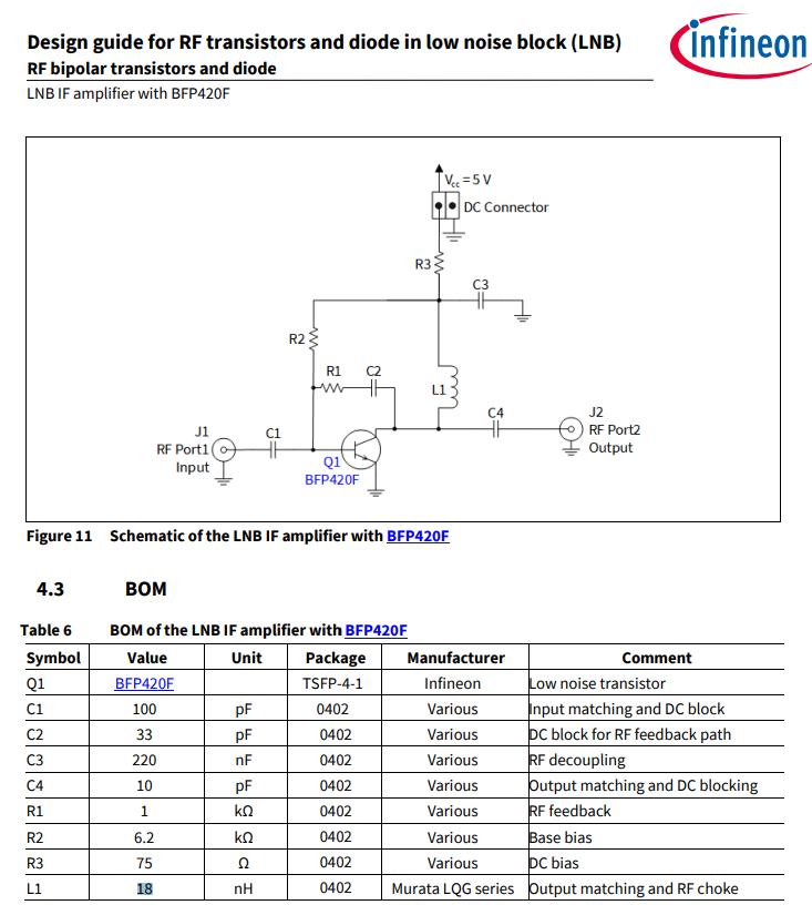 It’s kind of gratifying to see that both I and they converged on not really having any specific impedance matching components. I also decreased R2 a bunch which is also good to see. Let’s go ahead and switch out the components.
This is what I see (I gave up on using the attenuator):
It’s kind of gratifying to see that both I and they converged on not really having any specific impedance matching components. I also decreased R2 a bunch which is also good to see. Let’s go ahead and switch out the components.
This is what I see (I gave up on using the attenuator):
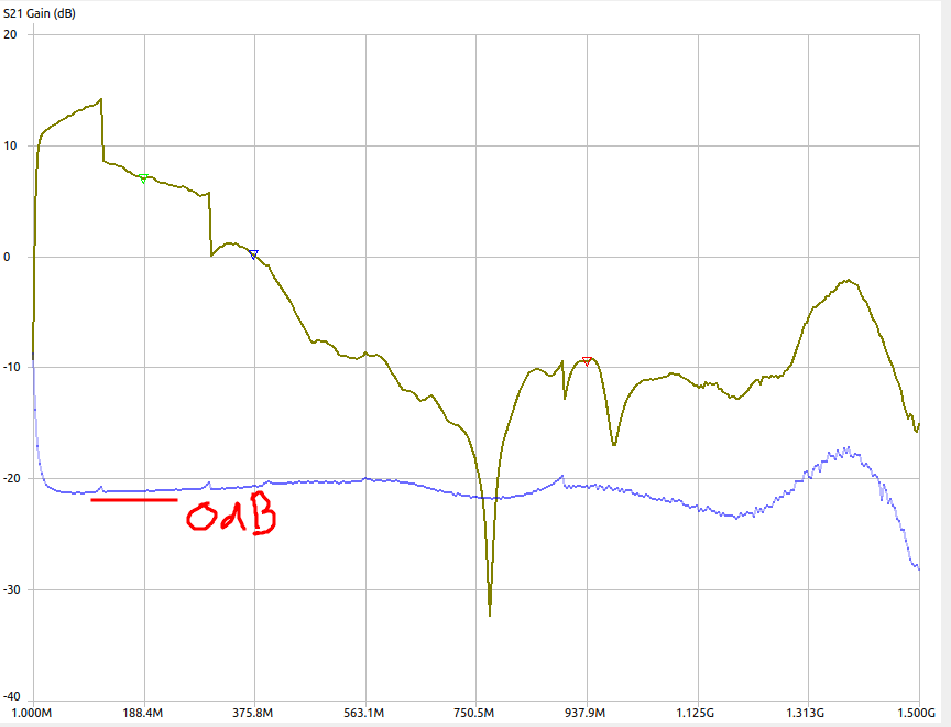
 As opposed to app note:
 Gee, that’s never happened before.
Oh wait it’s probably compression from the VNA’s high output amplitude. Setting 30dB of attenuation gets this:
Gee, that’s never happened before.
Oh wait it’s probably compression from the VNA’s high output amplitude. Setting 30dB of attenuation gets this:
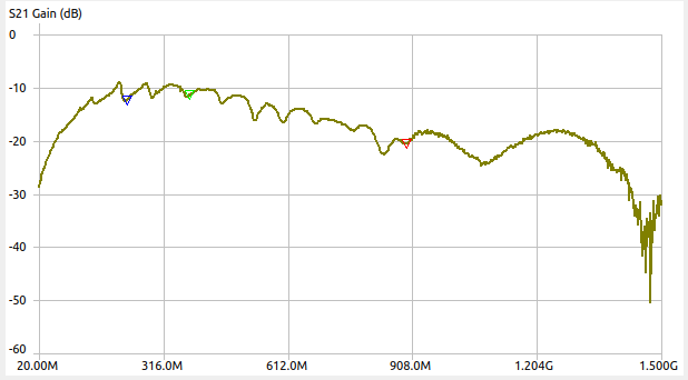 Which is much more reasonable, but also still only 10dB of gain.
That’s enough for today I think. I don’t know what to try next other than a different PCB layout, but I can’t help but think that’s not the problem.
Which is much more reasonable, but also still only 10dB of gain.
That’s enough for today I think. I don’t know what to try next other than a different PCB layout, but I can’t help but think that’s not the problem.
Small experiment
I tried measuring the gain with and without the supply decoupling cap and it made basically no difference. In retrospect this is not too surprising i suppose since there’s an inductor in line with the collector of the transistor but still this is evidence I suppose that the current layout is bad.
Inductor quality
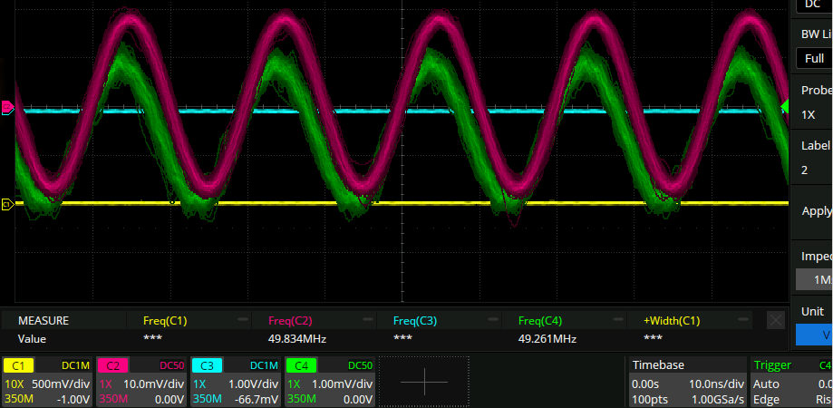
It’s quite possible that the inductor I am using on the collector of the transistor (L1 above) does not do well at 900MHz. So I made some handwound ones. Here is a 100nH one:
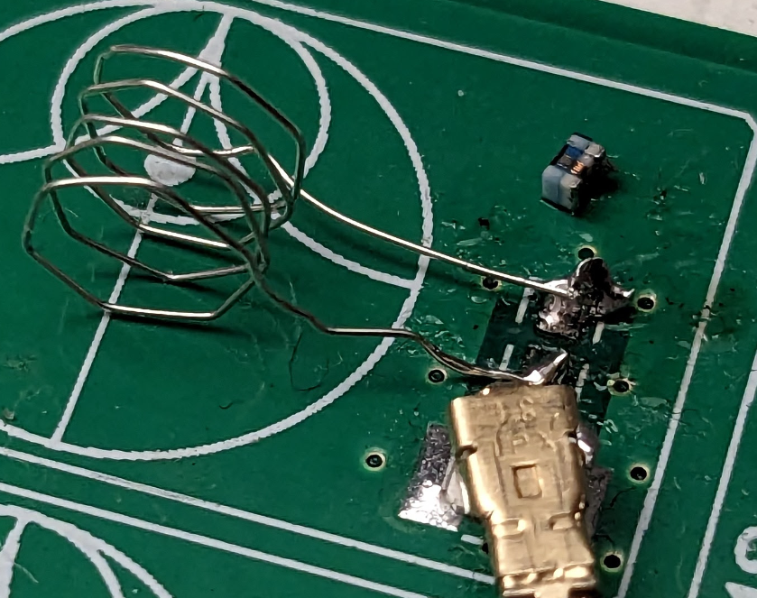 Blue is handwound 150nH, normal is 30nH chip inductor.
 So the inductors do seem to get a bit squiggly around 900MHz. When I attach various handwound inductors from 0 to 150nH the gain changes a tiny bit (1dB?) but not really that much.
Conclusion
Everything makes so little sense that I think I need to start from a known working example like an eval board. If even the most basic single transistor amplifier doesn’t work something is very wrong. The infineon eval boards are all “available on request”. Just give me the gerbers at least!!!